- Semiconductor BusinessHOME
- Products and Services of Macnica,Inc.
-
technical information

-
Events and Seminars
- Handling Manufacturer
- Support
- Inquiry
- Click here to purchase products
- Semiconductor business e-mail magazine registration


 Narrow down by specifying conditions
現在2183件がヒットしています。check
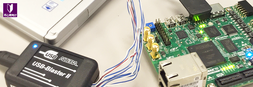

This page describes the Altera® FPGA development flow and provides information you should refer to at each development phase.
| First of all, what is an FPGA? I want to use FPGA, but I don't know where to start! If so, this article is a must-see! ▶ FPGA is a magic box! <Honto no Honto Introduction> ▶ Part 1. Creating an environment to start FPGA development ▶ Part 2. What to prepare to start FPGA development ▶ Part 3. Necessary knowledge to start FPGA development ▶ Part 4. Flow of FPGA development ▶ Part 5. Introduction of useful content |
| To develop Altera® FPGAs, use the Quartus® Prime design software. If you want to easily understand the basic operations of Quartus® Prime, you can learn it with this tutorial. ▶Quartus Prime Quick Tutorial Our popular hands-on seminars are now available online! You can take the course anytime, anywhere, at your own pace. ▶"Quartus® Prime Introductory Trial" video revealed! ▶"Nios® II Introductory Trial" video now available! ▶"SoC Startup Trial" revealed in video! ▶"Altera® HLS Introductory Trial" video now available! |
Altera® FPGA Development Flow Diagram
Altera® FPGA development proceeds as shown in the diagram below. To jump to each development phase, click the corresponding number.










(Click the appropriate number to jump to each development phase.)
1. Preparation
Download / Install / License setup
2. Examination of functional specifications
FPGA selection / configuration / power supply & power consumption estimation / board simulation
3. Logic circuit design
IP Information / Nios® II Information / SoC FPGA Information / OpenCL™ Information
Information on High Level Synthesis (HLS) / New to HDL design
4. Logical simulation
5. Constraint setting
6. Compile
7. Timing Verification
8. Programming
9. Actual equipment verification
10. Mass production
1. Preparation
Confirmation of correspondence status
Before proceeding with FPGA / CPLD design and development, let's find out what development environment you should prepare.
| The development software you use will vary depending on the FPGA/CPLD function you are developing and the device you are using. Incidentally, development software is sometimes called a "tool." Be sure to check the OS of the PC on which you will install the tool and the memory capacity it will have in advance. <Support table> ▶ Quartus® Prime - Windows® OS Support / Operating System Support (External site: Altera) ▶ Quartus® Prime - Supported Devices Compatibility Chart |
| The amount of memory required for your PC will vary depending on the FPGA/CPLD you are developing. Details are provided in the release notes. (You can easily find them by searching for "Memory Recommendations" within the release notes.) <Release Notes> ▶ Quartus® Prime Pro Edition Release Notes (External site: Altera) ▶ Quartus® Prime Standard Edition Release Notes (External site: Altera) |
| There are two versions of Quartus® Prime: a paid version that requires a license and a free version that does not require a license. There are differences in the devices and features supported. <Edition Comparison> ▶ Quartus® Prime Edition Comparison (External Site: Altera) |
download

For information on downloading the tool, please see the following page.
▶ How to download Quartus® Prime development software and Questa* - Altera® FPGA Edition
install

After downloading the installation file (installer) for the tool you want to install, the next step is installation.
For instructions on installing each tool, please see here. (If you are using the Nios® II embedded processor, you will also need the Nios® II Software Build Tool (Nios® II SBT), but the Nios® II SBT will be installed automatically at the same time as the Quartus® Prime installation.)
▶ How to install Quartus® Prime development software and Questa* - Altera® FPGA Edition
▶ Altera® SoC FPGA Embedded Development Suite (SoC EDS) Installation Instructions ver.20.1
▶ How to install the Software Development Kit (SDK) for OpenCL™
License settings

Once you have installed the tools, get and set up your license file. (The free-to-use Quartus® Prime Lite Edition can be used without obtaining and setting up a license file.)
License file generation and renewal are performed by signing in to the Altera® website and accessing a dedicated site called the Altera FPGA Self-Service License Center.
■ For sign-in, see the information below.
▶ How to create a new Altera® account
▶ How to register for the Altera® FPGA Self-Service Licensing Center
■ See below for information on how to obtain a license file.
▶ How to obtain new licenses for Quartus® Prime, IP, and Questa* - Altera® FPGA Edition
▶ How to obtain Quartus® Prime, IP, and Questa* - Altera® FPGA Edition licenses during maintenance renewal.
▶ How to change the NIC ID (Host ID) associated with Quartus® Prime, IP, and Questa* - Altera® FPGA Edition licenses.
▶ How to issue (reissue) license files for Quartus® Prime, IP, and Questa* - Altera® FPGA Edition licenses with assigned NIC IDs.
▶ How to obtain and configure the Questa* - Altera® FPGA Starter Edition license file.
▶ How to obtain a license file for the Nios® V processor IP
■ See the information below for setting up the license file.
The license for Altera® FPGAs includes FIXED License and FLOAT License There are two types, but the setup method for each is different.
▶ Quartus® Prime licensing options
▶ How to configure fixed licenses for Quartus® Prime, IP, and Questa* - Altera® FPGA Edition
▶ How to configure FLOAT licensing for Quartus® Prime, IP, and Questa* - Altera® FPGA Edition
▶ How to configure the license for Arm® Development Studio (DS) for Altera® SoC FPGA Edition
2. Examination of functional specifications
Consider the specifications of the functions to be implemented in FPGA / CPLD, and create block diagrams and specifications. By doing some paperwork and using Quartus® Prime to create a simple design (digital logic circuit), we thoroughly consider whether the functionality we want to implement is feasible.
In addition, in order to build a highly reliable logic circuit, it is important to learn the basics of design techniques, which are key points in RTL design of FPGA / CPLD. Before designing a logic circuit, we will introduce articles that FPGA / CPLD users must see. (Since it is easy to impose timing constraints, we recommend synchronous design especially for FPGA/CPLD. Regarding timing constraints, 5. Constraint setting Please refer to the. )
[A Must-See for Beginners in RTL Design] Series Articles
▶ [A must-see for RTL design beginners] Differences between synchronous and asynchronous design
▶ [Must-see for Beginners in RTL Design] Impact on the System when Inputting Asynchronous Signals
▶ [A Must-See for RTL Design Beginners] Effects of Hazard Signals on Systems
Now, I would like to introduce some materials and articles that I would like you to check in advance before proceeding with the specific consideration of FPGA.
FPGA selection
▶ Device Selection: Product Specifications (External site: Altera)
▶ Device information (External site: Altera)
▶ PIN Information: PIN Connection Guidelines / Pinout (External Site: Altera)
▶ Various documents: (External site: Altera)
▶ Development kit information (external site: Altera)
configuration
▶ Configuring the FPGA
▶ Remote System Upgrade for Altera® FPGAs
▶ Active Serial Configuration Design & Debug Guidelines / FPGA Guidelines
Estimated Power Supply & Power Consumption
▶ FPGA Power Consumption Types and Calculation Methods
▶ Power & Thermal Design & Debug Guidelines/FPGA Guidelines
▶ Enpirion® related articles and resources
board simulation
▶ Substrate simulation (HyperLynx)
SI (signal quality)
PI (power quality)
Thermal
DRC (Design Rule Check)
3. Logic circuit design
Quartus® Prime supports design in hardware description languages (HDL) such as Verilog HDL, SystemVerilog, and VHDL, as well as schematic design. Quartus® Prime also allows mixing HDL and schematics in the same project.
To begin FPGA/CPLD development with Quartus® Prime, you must first create a project. After creating the project, we will create the design (digital logic circuit) in HDL and circuit diagrams, but if you want to design in circuit diagrams, please refer to the following materials.
Getting Started with Quartus® - Material for Beginners
▶ Quartus® Prime - How to create a project
▶ Quartus® Prime - Using the Schematic Editor
Quartus® Step-Up Guide - Material for Intermediate Users
▶ Quartus® Prime - Managing Projects
▶ Quartus® Prime - Device Migration
▶ Quartus® Prime - Using the Qsys System Integration Tool
* Qsys from Quartus Prime v17.1 Platform Designer has been renamed to
IP information
Altera® and third parties provide various Intellectual Property (IP) for FPGAs. Please refer to this page if you are using IP.
▶ What is Altera® FPGA IP? (External site: Altera)
<PLL>
▶ Altera® FPGA PLL (← Check this page to see which PLL section you are referring to)
IOPLL edition / Altera PLL edition / ALTPLL edition
<External Memory Interface>
▶ DDR memory controller implemented in Altera® FPGA!
EMIF Design & Debug Guidelines / FPGA Guidelines
EMIF Layout Guidelines/FPGA Guidelines
DDR4 / DDR3
<PCI Express>
▶ PCI Express with Altera® FPGAs
PCI Express Design & Debug Guidelines / FPGA Guidelines
Avalon-ST Edition / Avalon-MM Edition
<JESD204>
▶ JESD204B on Altera® FPGAs
<HDMI>
▶ Easily display 4K video using HDMI 2.0 IP on Arria® 10 FPGA
Information on Roos® II / Roos® V
If you are implementing the Nios® II / Nios® V processor in your design, please refer to these documents and articles.
▶ Altera® FPGA Nios® II Processor
▶ Altera® FPGA Nios® V Processor
▶ Nios® V Processor What is it? (External site: Altera)
SoC FPGA Information
If you are using an Arm® core-integrated SoC FPGA, please refer to these documents and articles.
▶ Altera® FPGA SoC FPGA
OpenCL™ Information
If you are using the Intel® FPGA SDK for OpenCL™, please refer to these resources and articles.
▶What is Intel® FPGA SDK for OpenCL™? (External site: Intel)
Information about High Level Synthesis (HLS)
If you are using the Altera® HLS compiler, please refer to these documents and articles.
▶ HLS compiler for Altera® FPGAs
▶ Altera® HLS Compiler What is it? (External site: Altera)
New to HDL design
If you don't know how to write a hardware technology language (HDL), we have prepared content that you can learn with textbooks and exercises. If you learn this, you will be able to write a minimum description. Please take a look.
▶ Let's start! Verilog HDL <with exercises>
▶ Let's start! VHDL <with exercises>
4. Logical simulation
Once the design is complete, logical verification is performed using logic simulation. The simulation uses an RTL simulator such as ModelSim® - Altera® FPGA Edition, but the schematics supported by Quartus® Prime are not supported by RTL simulators. For instructions on converting Quartus® Prime schematics to HDL, please refer to "Quartus® Prime - Using the Schematic Editor".
▶ Altera® FPGA Functional Simulation with NativeLink (Standard Edition, Lite Edition)
▶ How to perform function simulation on a design containing IP generated with Quartus® Prime Pro Edition using Questa* - Altera® FPGA Edition (for Pro Edition)
<Quartus®Getting Started Guide> -Materials for beginner users
▶ ModelSim® - Altera® FPGA Edition - RTL Simulation Method
ModelSim/Questa
For mid-range and higher FPGA development, we recommend Questa or ModelSim for their fast simulation speed.
▶ RTL Simulator & Debug Tool / Questa / ModelSim
5. Constraint setting
After the RTL simulation is finished, pinouts, device settings, and various constraints are applied. Before compiling, be sure to make the necessary settings and constraints.
<Quartus® Beginner's Guide>-BeginnerMaterials for users
▶ Quartus® Prime - How to set device options
▶ Quartus® Prime - How to make pin assignments
▶ Quartus® Prime - Timing Constraint Methods
<Quartus® Step-up Guide>- IntermediateA user materials for
▶ Quartus® Prime - How to set up the EDA tool
▶ Quartus® Prime - Constraint Method (Assignment Editor)
▶ Quartus® Prime - How to set common pin options
6. Compile
After completing various settings and constraints, compile. Full compilation performs logic synthesis, placement and routing, timing analysis, and creation of programming files. After compiling, be sure to check the compilation report.
<Quartus® Beginner's Guide>-BeginnerA user materials for
▶ Quartus® Prime - How to read the compilation report file
<Quartus® Step-up Guide>-Materials for intermediate users
7. Timing Verification
Check the timing analysis results at the same time as the compilation report. Timing analysis results on the compilation report are summary information only, use the TimeQuest Timing Analyzer to see detailed results.
<Quartus® Beginner's Guide>-BeginnerA user materials for
▶ Quartus® Prime - How to do Timing Analysis
< FPGA guidelines>
▶ Timing & Implementation Design & Debug Guidelines/FPGA Guidelines
8. Programming
At this point, you will be ready to debug on the actual device. To write data to the FPGA/CPLD or configuration device, launch the Quartus® Prime Programmer and write to the device via an Altera® FPGA download cable (such as USB-Blaster™ II or USB-Blaster™).
<Quartus® Beginner's Guide > Beginneruser Materials for
▶ Quartus® Prime - How to Program Devices
<Quartus® Step-up Guide>- Intermediateuser Materials for
▶ Quartus® Prime - Generate and Convert Programming Files
<For those who want to know more>
▶ Programming EPCQ devices via FPGA (JIC programming)
▶ Installing the USB-Blaster™ II driver
▶ Installing the USB-Blaster™ driver
▶ Change the TCK frequency of the USB-Blaster™ II
9. Actual equipment verification
If the evaluation board is powered on again and the data is successfully transferred from the configuration device to the FPGA, it enters the phase of verifying the operation of the FPGA.
Getting Started with Quartus® - Material for Beginners
▶ Using the Quartus® Prime - Signal Tap Logic Analyzer
<Those who want to know more>
▶ Let's try FPGA on-chip debugging "Signal Tap"
* SignalTap®II from Quartus Prime v17.1 Signal Tap has been renamed to
10. Mass production
Once the actual machine verification is completed, we can move to mass production.
Recommended information
Article/Material
<FPGA Guidelines>
Articles and materials related to FPGA guidelines