- Semiconductor BusinessHOME
- Products and Services of Macnica,Inc.
-
technical information

-
Events and Seminars
- Handling Manufacturer
- Support
- Inquiry
- Click here to purchase products
- Semiconductor business e-mail magazine registration


 Narrow down by specifying conditions
現在2195件がヒットしています。check

Hello. I'm Hanako Altera, who provides technical support for Altera® FPGA products at Macnica.
The user designs the logic circuit inside the FPGA from scratch. Therefore, it is impossible to design without knowing anything at all.
So what exactly should we learn?
Note: Intel's Programmable Solutions Group became Altera®, an Intel company, in January 2024.

For now, let's start by learning about this.
- Knowledge of digital logic circuits
- Ability to code with hardware description languages
- Knowledge of I/O standards
- Knowledge of static timing analysis (STA: Static Timing Analyzer)
If you know more, it will be more convenient, but you can start designing if you know this area first.
Let's talk a little bit more about each.
Knowledge of digital circuits
FPGAs design digital circuits. By the way, in the FPGA industry, it is common to call a digital circuit a logic circuit.
To configure the logic circuit,
- Basic logic circuits such as AND, OR, NOT, and flip-flops
- Binary numbers, binary arithmetic
- combinational, sequential (flip-flop) circuits
- Synchronous sequential circuit, asynchronous sequential circuit
If you study about this area, you can design a basic circuit. (If there is a request from everyone, I will also write a technical article around here.)
Ability to code in a hardware description language
Coding ability of hardware description language is required to design logic circuits. The hardware description language is commonly known as HDL (Hardware Description Language), and currently the following three types are mainly used.
- VHDL
- Verilog-HDL
- SystemVerilog
Users usually design using one of them. (The characteristics of each will be introduced on another occasion.) It is up to the individual to choose which type of language. Some people are decided by the company, and some people master both languages in order to use them according to the order of the design client. Write the logic circuit you want to implement in those languages.
Learn basic grammar first. After that, please get used to “expressing logic circuits in language” by imitating sample circuits. Learning the grammar of a language is not that difficult. Rather than that, you may be more worried about how to express the logic circuit you want to realize in a language.
Language design does not describe the smallest unit of gate logic such as AND, OR, and flip-flops as in schematic (circuit diagram) design, but describes “circuit behavior” on a slightly larger scale.
For example, Figure 1 shows a 4-input 1-output multiplexer (selector) configured with gates.
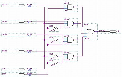
On the other hand, the same circuit written in VHDL looks like this.
Library ieee; use ieee. std_logic_1164.all; entity mux4to1 is port ( data :in std_logic_vector (3 downto 0); sel :in std_logic_vector (1 downto 0); q:out std_logic ); end mux4to1; architecture logic of mux4to1 is begin process (data,sel) begin case sel is when "00" => q <= data(3); when "01" => q <= data(2); when "10" => q <= data(1); when others => q <= data(0); end case; end process; end logic;There are no AND or NOT gates like in Figure 1, right?
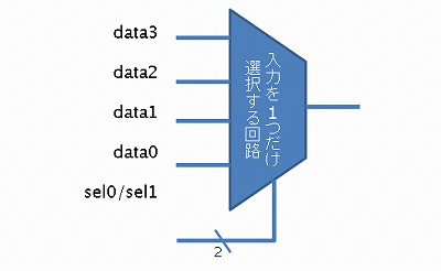
When you hear the word “4-input, 1-output multiplexer,” the image below probably comes to your mind first. The user describes what kind of input they want to operate (output) and let Quartus® Prime think about the gate configuration inside the box. This is language design!
If you refer to a book or site for learning logic circuit design, please look at the one that assumes designing in a language. Otherwise, even though we use a language that allows us to write logic circuits efficiently, we end up with an inefficient design that uses circuit symbols (AND and OR) to represent the logic as formulas. Studying the basics is important, but that is not what is required in practice. It is important to say, “Creating things (logic circuits) that move”.
But first, familiarize yourself with the language. To get you started, let's take a look at our free training content.
| training course name | Overview |
| Let's start! VHDL Let's start! Verilog-HDL [Japanese/free/with exercises] |
This page is for those who are designing hardware logic circuits in VHDL or Verilog-HDL for the first time. You can learn from the basics of the basics, and you can practice and deepen your understanding. |
There is another use of the hardware description language besides describing logic circuits. It is used to describe a “language for executing simulation (operation verification) of the described logic circuit”, a so-called “testbench”.
For simulation, please see the following page.
For testbench description, see the following page.
Knowledge of I/O standards
FPGA is a digital IC. Determines whether the signal (received) input to the I/O pin is "High (1)" or "Low (0)" and outputs (transmits) the signal to the connected IC. By doing so, it determines whether it is "High (1)" or "Low (0)" and communicates with the peripheral device. Even if you say high and low in one word, the voltage value is actually related on the board. The I/O standard is the name given to each voltage value range, such as "a certain volt (V) or more is high, and a certain volt or less is low".
There are various types of I/O standards, and currently Altera® devices support a variety of I/O standards, including single-ended and differential standards (see the figure below for some examples). However, not all families support all of the following, so please check the handbook for each family.
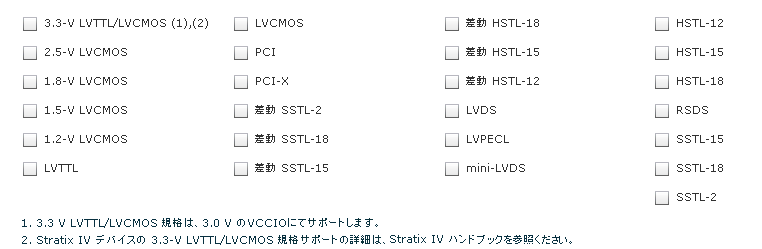
The concept of "a voltage above a certain volt (V) is high and below a certain volt is low" is the idea of a single-ended standard. or Low. Single-ended standards include LVTTL and LVCMOS. Among the single-ended standards, there are also standards that supply an external reference voltage and determine whether it is High or Low based on the difference from the reference voltage.
LVDS, LVPECL, etc. are differential standards. The voltage difference between the two signals determines whether it is high or low depending on whether it is above or below a specified value.
When developing an FPGA with Quartus® Prime, you assign the input, output, and bidirectional pins of the created logic circuit to each pin of the target device. At that time, you can optionally set not only the pin number but also which I/O standard you want each pin to comply with. Therefore, users should be aware of the characteristics of the required I/O standard.
FPGAs can support multiple I/O standards on a single chip. This is because FPGAs have separate power supplies for internal operation (commonly known as core power supplies) and power supplies for I/O terminals to communicate with external devices (commonly known as I/O power supplies). The area (group) of I/O pins that can be driven by each I/O power supply is called an “I/O bank”, and Altera® FPGAs have multiple I/O banks on a single chip. Because different power supply voltages can be supplied to each I/O bank, FPGAs can connect to various peripheral devices with different I/O standards on a single chip.
Users must determine the I/O standard of the peripheral device to be connected to the FPGA, check the electrical characteristics of the I/O standard, and select an FPGA family that can support the I/O standard. Users must also download the data sheet of the FPGA they have selected (or will select) from the Altera® website and check the DC characteristics of the inputs and outputs.
Knowledge of static timing analysis (STA: Static Timing Analyzer) and timing constraints
Timing analysis is to check whether the logic circuit you created operates "correctly" at the required clock frequency, and other timing specifications are satisfied. In contrast to simulation, which uses a simulator such as QuestaSim to simulate the operation of a circuit using input signal data (also called test patterns or test benches), a method that does not use test patterns but analyzes (compares and verifies) against timing requirements (constraints) set by the user is called "static timing analysis."
FPGA circuit elements have inherent delays, so if the required clock frequency is high or the scale of the logic circuit is large, part of the logic circuit may not work. Therefore, we have to perform timing analysis and confirm that it works correctly according to the specifications. It is no exaggeration to say that if timing analysis is neglected, it is not an exaggeration to say that FPGA will not work on the actual device. STA is one of the important tasks in current FPGA development.
Timing requirement information (timing constraints) for the user's circuit is essential for static timing analysis. By instructing the timing constraints to the FPGA development tool Quartus® Prime, the tool executes logic synthesis and placement and routing (so-called “compilation”) using these as target values. Quartus® Prime uses the “SDC (Synopsys Design Constraints)” file format for timing constraints, which is standard in ASIC development.
An example of the most basic timing constraint is specifying the clock frequency. Besides this, various constraints are necessary depending on the design requirements. For example, the input/output pins of FPGA (user circuit) require delay constraints for input/output data, and if there are multiple clocks in a logic circuit, it is necessary to define the correlation between the clocks as a constraint. Write its contents to the SDC file.
You don't have to worry about "Do I have to learn SDC in addition to writing logic circuits in HDL?" SDC doesn't have to be learned from scratch like an HDL language. The development software Quartus® Prime has a dedicated editor for writing timing constraints (SDC), and you can easily write commands by entering the necessary information in the prepared dialog Box.
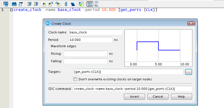
However, before writing SDC, you need to understand the basic concepts of timing (such as setup time and hold time). If you don't know this, you won't know what kind of constraints to write, and you won't get correct analysis results unless you provide appropriate timing constraints according to the circuit structure.
Timing analysis is an essential step in FPGA design. Learn about timing constraints and analysis to ensure a properly functioning product.
Hanako's recommendation♪
An online seminar for beginners on timing constraints and analysis is currently being held.
For more information, please check the page below.
Information on Altera® FPGA Seminars/Technical Training
This time, I introduced roughly what kind of things you should study. Use this as an opportunity to gradually deepen your knowledge.
Next time, I will introduce the flow (procedure) of FPGA development.
Notes:
In this article, the Japanese page of the manufacturer's website is shown for the convenience of readers, but please be sure to check the English page as well. Please note that the Japanese page may be delayed in updating information. Language switching within the site can be done using REGION at the bottom of the page. Please note that even if you switch languages, not all pages will be in Japanese.
Click here for recommended articles
The real real introduction part 1.Creating an environment to start FPGA development
Honno Honno Introduction Part 2. What to prepare to start FPGA development
The real introduction 3. Necessary knowledge to start FPGA development
The real introduction part 4. Flow of FPGA development
The real introduction Part 5. Introduction of useful content