- Semiconductor BusinessHOME
- Products and Services of Macnica,Inc.
-
technical information

-
Events and Seminars
- Handling Manufacturer
- Support
- Inquiry
- Click here to purchase products
- Semiconductor business e-mail magazine registration


 Narrow down by specifying conditions
現在2240件がヒットしています。check

Hello. I'm Hanako Altera, who provides technical support for Altera® FPGA products at Macnica.
Now that the environment for FPGA development has been set up after proceeding from Part 1 to Part 3, it's time to put it into practice. This section describes how to proceed with the work (flow).

Note: Intel's Programmable Solutions Group became Altera®, an Intel company, in January 2024.
Flow of FPGA development
FPGA development involves roughly eight steps (steps 2-9 in the diagram below). Steps 3 and 5-9 are performed using Quartus® Prime, while step 4 is performed using an EDA simulator such as Questa* - Altera® FPGA Edition.
For operating manuals for the tools used in each step, please refer to the Altera® FPGA development flow page.










1. Preparation
Prepare the computer environment for using the FPGA development software Quartus® Prime and set up the development software.
Please refer to the following page for details.
Computer environment required for development
About setting up the development software
2. Examination of functional specifications
Based on the system specifications, consider the functions to be implemented in the FPGA (how to process them), and summarize them in specifications such as block diagrams, external interfaces, and inter-block interfaces.
Also, select a family of FPGAs that meets the specifications.
If you plan to use the specific internal features of the FPGA you intend to use, such as PLL (Phase Locked Loop), multiplier blocks, or RAM blocks, you should first use FPGA development software such as Quartus® Prime or Questa* - Altera® FPGA Edition to create a simple sample design or perform logic verification (RTL simulation) to confirm its operation.
3. Logic circuit design
The operation of logic circuits is described using HDLs (hardware description languages) such as VHDL, Verilog-HDL, and SystemVerilog. Design can also be done using dedicated schematic editors, but in recent years design using languages has become mainstream. These descriptions are mainly called "designs".
Although HDL can be written using a general-purpose text editor, the text editor built into Quartus® Prime is recommended because it has features not available in general-purpose text editors, such as the ability to insert templates and sample designs, and the convenient function of displaying characters in color according to grammar.
In addition, the size and speed of HDL circuits vary depending on how they are written, just like C programs. Quartus® Prime automatically optimizes user-created designs according to the architecture (structure) of the target device.
To use functional blocks (such as multipliers, memory, PLLs, transceivers, etc.) installed in FPGAs, use the Quartus® Prime IP Catalog tool. Select a dedicated block that is already available in the IP Catalog, and customize it by selecting and changing the port configuration and parameters. After that, generate a file and connect it to your design and incorporate it. (IP: Altera® FPGA Intellectual Property)
For information about Altera® FPGA Intellectual Property, please see below.
4. Logical simulation

To verify whether the designed logic circuit (design) meets the user's specifications, the logical operation is checked on a PC using a simulator such as Questa* - Altera® FPGA Edition.
The method of checking the simulation execution results is mainly to use graphically displayed waveforms. If there are operating points that differ from the specifications, it means that the description of the designed logic circuit is incorrect, so correct the description. , and check the behavior again in simulation. Repeat this process to complete the description of the logic circuit.
At this time, input signal data (also called test pattern or test bench) to the verification target circuit is required in addition to the design of the logic circuit realized by FPGA. The testbench allows the user to write test pattern information according to specifications in HDL language and load it into the simulator.
Since the testbench is written by the user, if this input pattern is different from the specification, the verification itself will be a waste of work.
If you are new to HDL design, please refer to sample sources such as reference books when writing.
Please refer to the following article for the description of the testbench.
5. Constraint setting
In FPGA development, the user does the pin layout of the device themselves.
Depending on the placement environment of the FPGA and peripheral devices on the board, determine the location of the pins on the FPGA side so that the wiring is short.
Also, FPGA pins have various built-in functions, such as the ability to change the output pin drive current, internal pull-up resistors, and the ability to enable internal termination resistors. Applying the pin function to the device is accomplished by setting options and compiling in Quartus® Prime.
In addition, the operating speed of the FPGA is also set by the user as a timing constraint. Unlike ASSPs, which have fixed operating frequencies, FPGAs rely on the configuration of user-created logic circuits. Of course, there is a limit to the speed of FPGAs, so at the stage of considering adoption, it is necessary to select a family that has specifications such as the clock frequency to be introduced and the data transfer speed with peripheral devices that can be achieved, but the desired timing By setting conditions, the Quartus® Prime Compiler will realize the optimal gate configuration and placement.
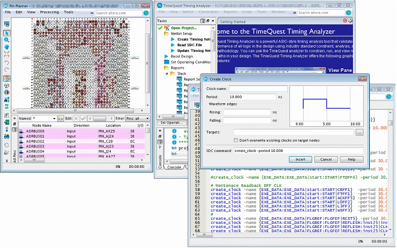
These constraints need to be set and input in Quartus® Prime before compilation (logic synthesis and place-and-route). Graphical tools such as Pin Planner: left) and Timing Analyzer (timing analyzer: right) are used. Timing constraints are in the SDC format, which is standard in ASIC design. A wizard for creating the SDC code is also provided as an auxiliary function, so users who do not know the SDC format can easily describe timing constraints.
6. Compile
After creating the design and setting various constraints, execute “Compile”.
Compilation is a general term for work that mainly performs "logical synthesis" and "placement and routing". Quartus® Prime initiates these tasks by simply clicking an icon on the screen, and then automatically performs them.
“Logic synthesis” is the work of converting a design created by the user in an HDL description language or a schematic into concrete gate circuits such as ANDs and flip-flops, which conforms to the structure of the FPGA used by Quartus® Prime. Automatically converts with the optimal gate configuration.
After that, according to the structure of the FPGA to be used, internal logic placement and pin positions are determined as specified by the user, and routing is automatically performed between logic and between logic and pins. This is called “place and route”.
When the compilation is finished, the results of various compilation processes are generated as a report, and the contents can of course be checked using the GUI.
7. Timing Verification
The compilation report also contains timing analysis results.
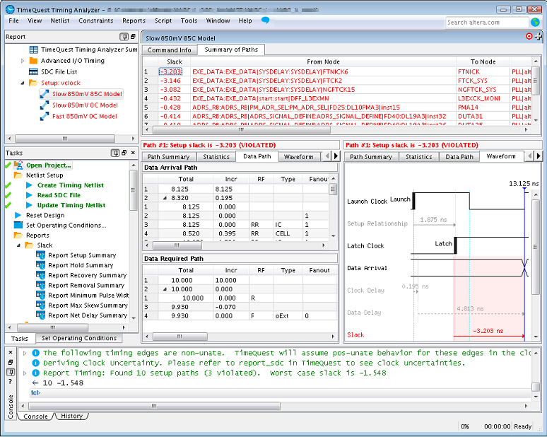
The user must confirm whether the circuit implemented in the device operates at the required speed (whether the required values set by the timing constraints are met). Timing analysis results in the compilation report are only summary information, so to see detailed results, use the Timing Analyzer in Quartus® Prime and verify statically.
If the results do not satisfy the required values, use the Quartus® Prime options to change the placement and routing algorithm, apply the device functions, and recompile to change the internal layout. We will try to improve by doing so.
8. Programming
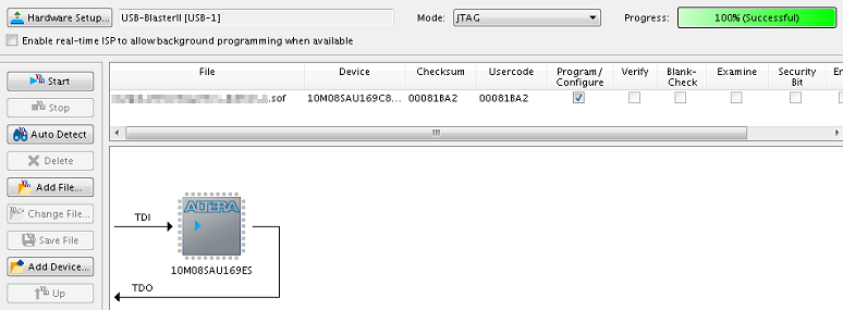
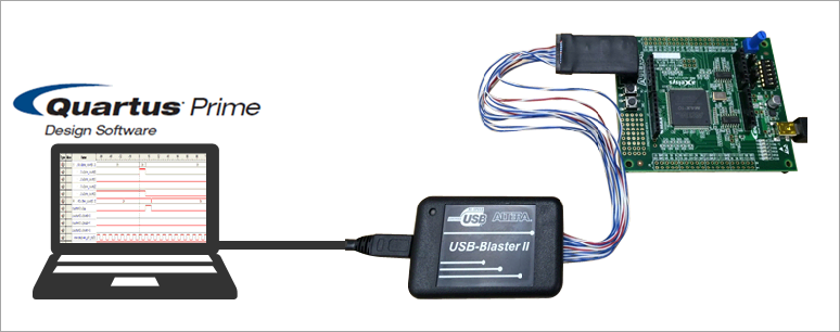
After the timing analysis shows that the circuit works correctly as requested by the user, the circuit data generated by Quartus® Prime is transferred from the personal computer to the FPGA in order to actually operate the FPGA on the development board. This is called “programming” (also known as downloading).
Users can program the FPGA using the Altera® FPGA download cable USB-Blaster™ II and a utility called Programmer that comes with Quartus® Prime.
Many FPGAs use SRAM as a program element, so a non-volatile memory for boot memory must be prepared on the board. Altera® calls the non-volatile memory device "configuration ROM" and programs this memory. The FPGA only operates when data is transferred from this configuration ROM on the board. This is called "configuration".
The only exception is the MAX® 10 FPGA family. MAX® 10 is a new type of FPGA that has a built-in boot memory on a single chip. Therefore, MAX® 10 does not require an external boot memory.
9. Actual equipment verification
After powering the board back on and successfully transferring data from the configuration ROM to the FPGA, we move on to the phase of verifying the operation of the FPGA.
When there is a malfunction, signal verification is generally performed with a logic analyzer or oscilloscope, but for simple signal verification, Quartus® Prime has an on-chip debugging function called Signal Tap. This is a debugging method (mechanism) that configures a logic analyzer inside Altera® FPGA, and does not require any special equipment. All you need is a PC with Quartus® Prime installed, a board with the FPGA to be verified, and a download cable USB-Blaster™ II, and you can start debugging right away. SignalTap can be used without a license and can also be used with the free Quartus® Prime Lite Edition.
If you want to know more about Signal Tap or want to try it, please see the article below.
For more details on Signal Tap, please refer to the manufacturer's documentation below.
- Design Debugging with the Signal Tap Logic Analyzer (Quartus Prime Standard Edition)
- Design Debugging with the Signal Tap Logic Analyzer (Quartus Prime Pro Edition)
10. Mass production
Mass production can be started as soon as the actual machine verification is completed.

The above is the general flow of FPGA development.
Let's give it a try!
However, if you have no experience with FPGA development, it would be foolhardy to start by coming up with specifications. Let's start by imitating it.
Evaluation boards released by Altera® and Mpression (Macnica 's original brand) come with reference designs (sample designs) and user guides (manuals). You can download sample design data from the evaluation board listing page on the website before or after purchase, or even if you don't purchase the board.
There are other ways to get sample designs other than the evaluation board page. For details, please see the content below.
Even if you do not yet have an evaluation board on hand, you can immediately begin steps 3 to 7.
First, get familiar with how to use the tools.
It is no exaggeration to say that mastering Quartus® Prime is the shortcut to FPGA development.
To get up and running quickly, we recommend instructor-led training.
If you have any questions, please contact our staff or use the inquiry form for semiconductor products.
This series of "The Real Introduction" will end in the next installment. In the final installment, "Part 5," I will introduce some useful websites for studying FPGAs and CPLDs.
Notes:
In this article, the Japanese page of the manufacturer's website is shown for the convenience of readers, but please be sure to check the English page as well. Please note that the Japanese page may be delayed in updating information. Language switching within the site can be done using REGION at the bottom of the page. Please note that even if you switch languages, not all pages will be in Japanese.
Click here for recommended articles
Real real introduction part 1. Creating an environment to start FPGA development
Honno Honno Introduction Part 2. What to prepare to start FPGA development
The real introduction 3. Necessary knowledge to start FPGA development
The real introduction part 4. Flow of FPGA development
The real introduction Part 5. Introduction of useful content