- Semiconductor BusinessHOME
- Products and Services of Macnica,Inc.
-
technical information

-
Events and Seminars
- Handling Manufacturer
- Support
- Inquiry
- Click here to purchase products
- Semiconductor business e-mail magazine registration
![]()
![]() Narrow down by specifying conditions
Narrow down by specifying conditions
現在2189件がヒットしています。check

This article explains how to implement PCI Express in an FPGA. One example is the Avalon Memory Mapped (Avalon-MM) configuration. This article explains how to verify operation using the PCI Express Avalon-MM configuration sample design on an Arria® 10 FPGA.
By using this reference design, you can easily check that the target PC and board environment works. By changing the device model number and pinout, you can also use it to check operation on your own board.
environment
- Tools: Quartus® Prime Design Software v17.1
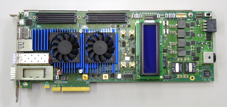
- Development Kit: Arria® 10 GX FPGA Development Kit < Macnica-Mouser Purchase Site >
- PC: Desktop PC with PCI Express interface
- OS: Windows®7, Windows®10
* The Qsys system integration tool has been renamed to Platform Designer starting with Quartus Prime v17.1.
procedure
- Introduction to reference designs
- Reference Design 1: Gen2, 8 lane configuration, no external memory connection
- Reference Design 2: Gen3, 4 lane configuration, no external memory connection
- Reference Design 3: Gen2, 8 lane configuration with external memory connection
- operation check
- Software installation
- Hardware settings
- operation check
- How to change the design
- Design considerations
- address_span_extender について
- Hard IP mode selection
1. Introduction of reference design
The design uses a DMA engine implemented inside the FPGA to perform DMA transfers. In the case of DMA read, when a command is issued via the PCI Express link by the operation from the PC software, the necessary information is set in the DMA engine configuration register and the DMA engine operates as the master. The DMA engine reads data from PC-side memory with memory read commands and writes data to on-chip memory inside the FPGA or to external DDR4 SDRAM memory connected to the FPGA. Conversely for DMA writes, the DMA engine reads data from on-chip memory inside the FPGA or from external DDR4 SDRAM memory connected to the FPGA and writes data to memory on the PC side with memory write commands. Write.
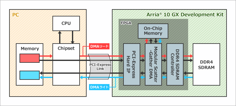
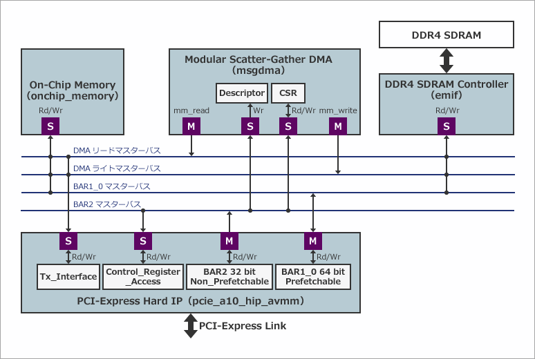
This design implements PCI Express Hard IP, on-chip memory, DMA engine, and external memory (DDR4 SDRAM) controller as Platform Designer components. PCI Express Hard IP is connecting with PCI Express Link. The base address implements a 64-bit prefetchable address space in BAR1_0 and a 32-bit non-prefetchable address space in BAR2. Contorol_Register_Access is a slave port for register access to make various settings for the bridge function, such as settings for converting between the address space of PCI Express (PC side) and the address space of Avalon-MM (Platform Designer side). increase. Tx_Interface acts as a slave port to accept requests from DMA read/write masters (mm_read/mm_write).
The on-chip memory becomes the transfer target when the transfer mode of the transfer rate measurement software is set to “Run OnChipMemory DMA Test”. The external memory controller becomes the transfer target when the transfer mode of the transfer rate measurement software is set to “Run DDR DMA Test”. In these modes, each target memory is accessed by PCI Express BAR1_0 masters and DMA read/write masters.
The DMA engine uses mSGDMA (Modular Scatter-Gather DMA). Platfrom Designer has two other types of DMA engines, DMA (Simple DMA) and SGDMA (Scatter-Gather DMA), but mSGDMA is suitable for DMA transfers that require a wide bandwidth.
Reference Design 1: Gen2, 8 lane configuration, no external memory connection
Example design with Gen2, 8-lane configuration and no external memory connection. You can check the operation immediately on the Arria® 10 FPGA development kit. Since there is no external memory connection, it can be easily ported to other boards.
For Gen2, 8 lanes, the theoretical total bandwidth is 4000MB/s. Take some margin and estimate the effective bandwidth to be 50 to 60% of the theoretical value (approximately 2000 to 2400MB/s).
a10_devkit_pcie_g2x8_msgdma_grd_17_1__1.qar
Reference design 1
Reference Design 2: Gen3, 4 lane configuration, no external memory connection
Example design with Gen3, 4-lane configuration and no external memory connection. You can check the operation immediately on the Arria® 10 FPGA development kit.
Even with Gen3 and 4 lanes, the theoretical total bandwidth is 4000MB/s. Take some margin and estimate the effective bandwidth to be 50 to 60% of the theoretical value (approximately 2000 to 2400MB/s).
a10_devkit_pcie_g3x4_msgdma_grd_17_1__1.qar
Reference design 2
Reference Design 3: Gen2, 8 lane configuration with external memory connection
Example design with Gen2, 8-lane configuration, and external memory (DDR4 SDRAM) connectivity. You can check the operation immediately on the Arria® 10 FPGA development kit. Since there is a function to connect to external memory, you can check the DMA transfer function to the external memory of the GUI software described later. Please use it as a reference design when mounting an external memory.
a10_devkit_pcie_g2x8_msgdma_ddr4_grd_17_1__2.qar
Reference design 3
operation check
Here, we will use the reference design 3 introduced above to introduce how to actually check the operation.
Software installation
First, download the GUI software for Windows® below.
https://fpgawiki.intel.com/uploads/e/e7/GUI_for_AN431.zip
Extract GUI_for_AN431.zip to a suitable folder and install the driver according to the contents of Readme.txt.
Hardware settings
First, attach the daughter card for DDR4 SDRAM to the HILO connector for external memory. Next, plug the board into your PC, connect the JTAG cable, and power on your PC.
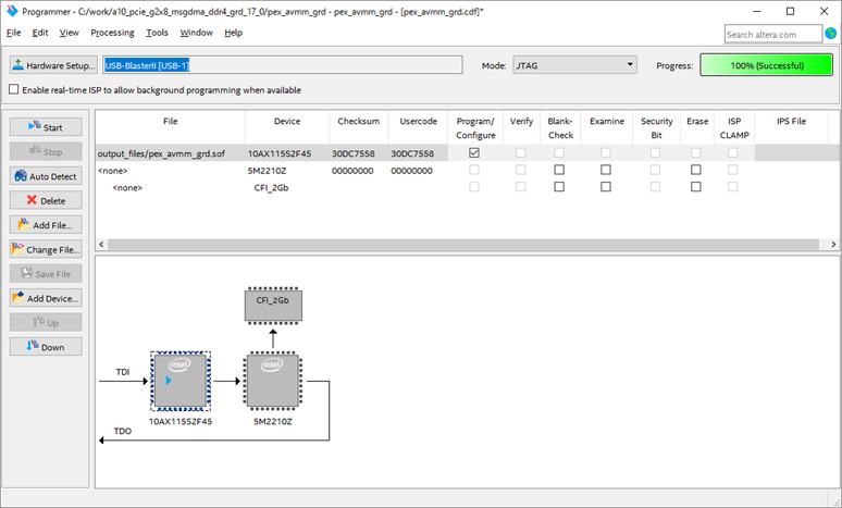
After the PC boots, extract the reference design3 to a suitable folder and open it with the Quartus® Prime software. Start Programmer and write SOF file. Once the burning is complete, restart your PC. Rebooting the PC initializes the communication between the root complex on the PC side and the endpoints in the FPGA.
operation check
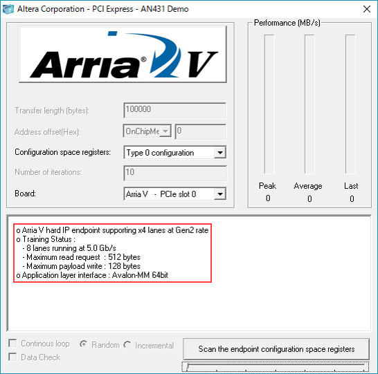
After the PC restarts, double-click altpcie_demo_Qsys_64.exe in the folder where GUI_for_AN431.zip is expanded. If you are using a 32-bit OS, run altpcie_demo_Qsys_32.exe.
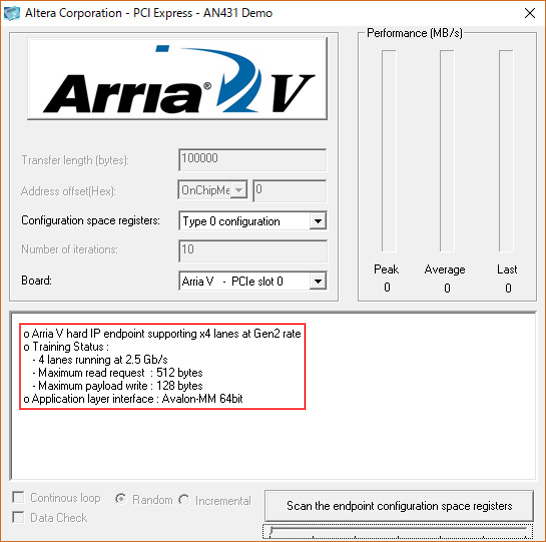
If you can link correctly, you will see "8 lanes running at 5.0Gb/s" as shown in the red frame. The device series is displayed as "Arria V", but the software has not been updated and there is no problem in operation, so proceed without worrying about it.
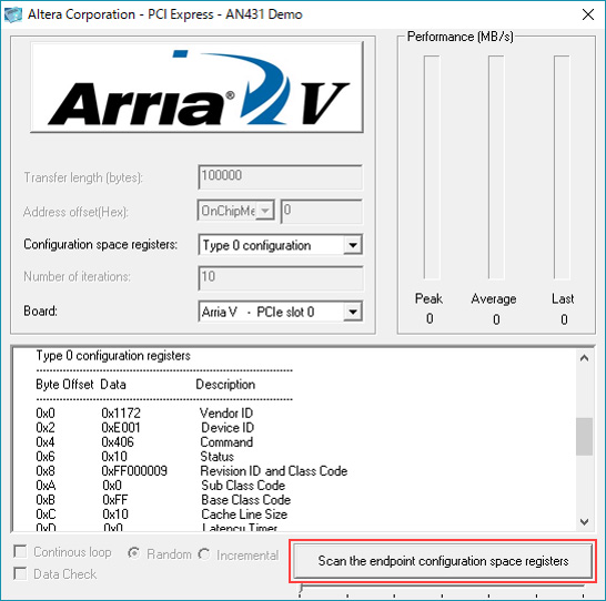
Clicking on "Scan the endpoint configuration space registers" will display the information of the connected endpoint's configuration space registers. 0x1172 is the old Altera device ID.
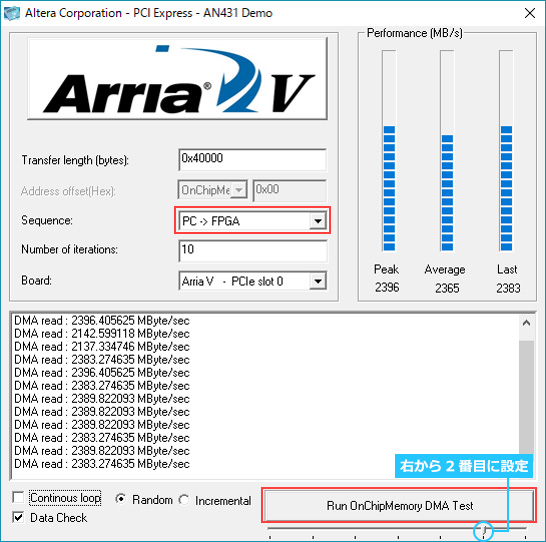
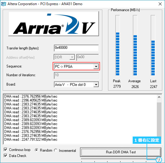
If you set the lower right slide bar to the second from the right (blue circle), it will be a DMA transfer mode targeting on-chip memory. Since Sequence is PC ⇒ FPGA, it will be DMA read. Click "Run OnChipMemory DMA Test" to start the DMA transfer. By default, it performs 0x40000 bytes of data transfer and displays Peak (highest value), Average (average value) and Last (last data).
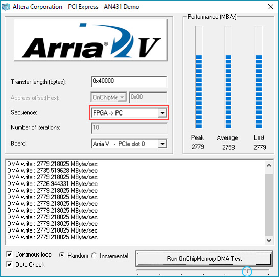
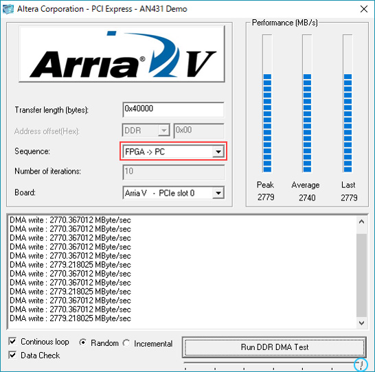
If Sequence is changed from FPGA ⇒ PC, DMA write will be executed.
Setting the bottom right slide bar to the far right (blue circle) will enable DMA transfer mode targeting external DDR4 SDRAM memory. Below is the result when executing a DMA read.
Below is the result when executing a DMA write.
How to change the design
The transfer rate and number of lanes in this design can be easily changed. The following describes how to change reference design 3 to 4 lanes of Gen1.
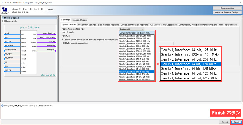
First, open pex_avmm_grd.qsys from Platform Designer, then open pcie_a10_hip_avmm. As shown, select "Gen1x4, Interface: 64 bit, 125MHz" and click the Finish button.
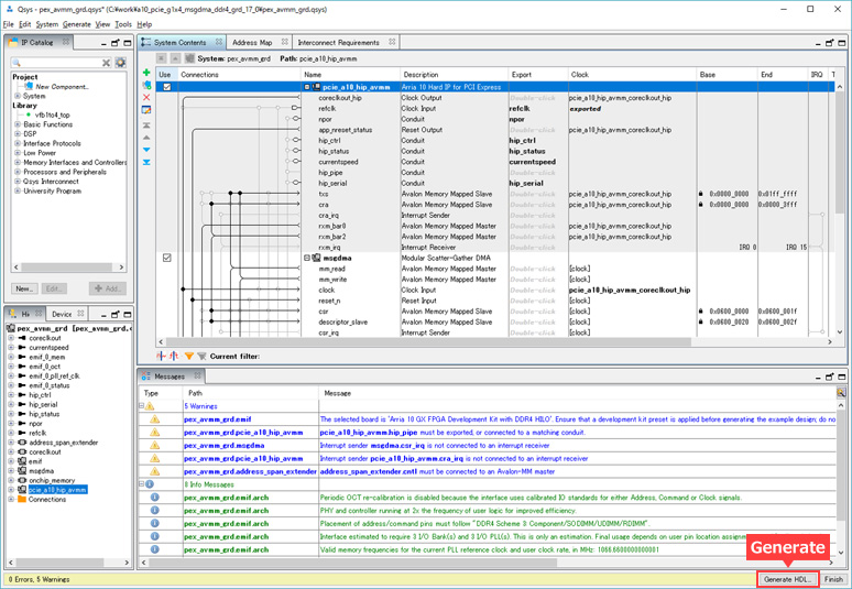
Generate Platform Designer.
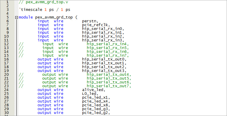
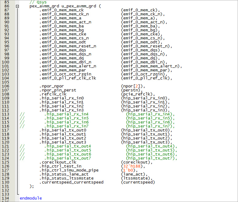
Next, edit the top file (pex_avmm_grd_top.v). Since we are changing from 8 lanes to 4 lanes, comment out all the descriptions for lanes 4 to 7.
Execute compilation and check the operation with the generated SOF file. If you can see "4 lanes running at 2.5Gb/s" on the GUI software, then you have edited it correctly.
Design considerations
address_span_extender について
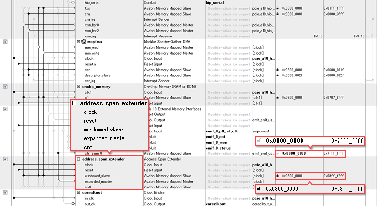
For Reference Design 3 with external memory, when you open pex_avmm_grd.qsys in Platform Designer, you can see that "address_span_extender" is implemented in the System Contents tab. The software GUI specifies the starting address of the external DDR memory as 0x08000000, so the base address of the DDR4 SDRAM memory in Platform Designer must also match 0x0800_0000. However, the address width of the DDR4 SDRAM memory implemented on this evaluation board is large, from 0x0000_0000 to 0x7FFF_FFFF (2GB), so if the base address is set to 0x0800_0000, Platform Designer cannot specify consecutive address values.
The address_span_extender is implemented as a measure to avoid this. The address of the windowed_slave of the address_span_extender is 32MB: 0x0800_0000~0x09FF_FFFF, so in reality, 32MB of the 2GB DDR4 SDRAM memory area is being accessed.
If you want to use this design to access large-capacity external memory, you can change the base address to a value such as 0x0000_0000, which will enable you to access a large address space without using address_span_extender.
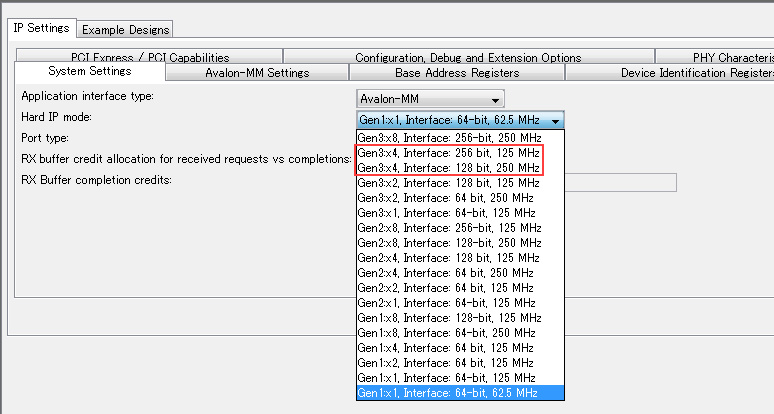
Hard IP mode selection
There are multiple options depending on the selected transfer rate and number of lanes. For example, for Gen3x4, you can select "Gen3x4, Interface: 256 bit, 125MHz" and "Gen3x4, Interface: 128 bit, 250MHz". This represents the bus width and speed (Fmax) of the generated Avalon bus. In the former case, the bus width is small but the speed is high. In the latter case, the bus width is large but the speed is high. This is a slow configuration.
There is no problem functionally with either choice, but the former tends to have a tighter timing met. The latter case consumes more device resources. Please consider the above and make a selection.
User guide
Arria 10 and Cyclone 10 Avalon Memory-mapped Interface for PCIe Design Example User Guide
Stratix V Avalon-MM Interface for PCIe Solutions User Guide
Arria V Avalon Memory-Mapped (Avalon-MM) Interface for PCI Express Solutions User Guide
Cyclone V Avalon Memory-Mapped (Avalon-MM) Interface for PCI Express Solutions User Guide
Click here for recommended articles/materials
PCI Express with Altera® FPGAs
PCI Express with Altera® FPGA (Avalon-ST Edition)
FPGA PCI Express Design & Debug Guidelines
Altera® FPGA Development Flow