- 半導体事業HOME
- マクニカの製品・サービス
-
技術情報

-
イベント・セミナー
- 取扱メーカー
- サポート
- お問い合わせ
- 製品購入はこちら
- 半導体事業のメルマガ登録
![]()
![]() 条件を指定して絞り込む
条件を指定して絞り込む
現在2182件がヒットしています。check

こんにちは。マクニカで Altera® FPGA 製品の技術サポートをしている 鷲宮タロー です。
『PLL』で FPGA の PLL の概要を解説しましたが、ここでは IOPLL を使用するための手順について解説します。
なお、IOPLL を使用できる FPGA ファミリーは『PLL』で確認できます。
内容
使用するツール
- Altera® Quartus® Prime Pro Edition 開発ソフトウェア
- ModelSim® - Altera® FPGA Edition
ターゲットの FPGA と開発ツールのエディションの関係については、Quartus® Prime のエディション比較 をご覧ください。
開発ソフトウェアのインストールが済んでいない方は、Altera® FPGA の Web サイトから入手できます。
詳細は、下記コンテンツをご覧ください。
Altera® Quartus® Prime 開発ソフトウェアおよび ModelSim® - Altera® FPGA Edition のダウンロード方法
Altera® Quartus® Prime 開発ソフトウェアおよび ModelSim® - Altera® FPGA Edition のインストール方法
1. IOPLL の生成
ここでは、Cyclone® 10 GX のプロジェクトを例に説明します。
ターゲットデバイスが Cyclone® 10 GX のプロジェクトを開くか、新規にプロジェクトを作成します。
(Quartus® Prime のプロジェクト作成は、Quartus® はじめてガイド - プロジェクトの作成方法 を参照してください。)
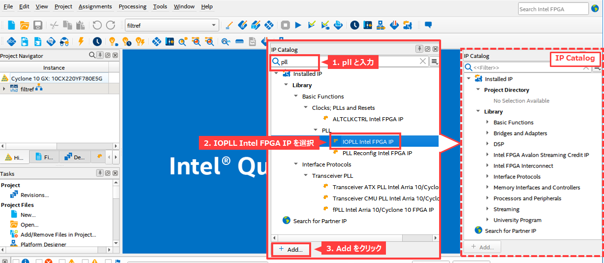
Quartus® Prime 内の IP Catalog の検索バーに pll をタイプ入力してください。
すると、IOPLL を容易に探し出すことができます。
IOPLL をハイライトした状態で、Add をクリックします。
IP Parameter Editor が起動します。
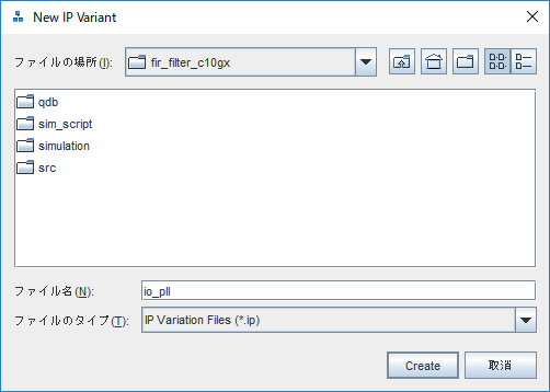
IOPLL を生成するフォルダーパスと、作成する IOPLL に付ける名前を指定して、Create をクリックします。
IP の生成先は、プロジェクトの作業フォルダーか、その下位フォルダーを指定することをお勧めします。
IOPLL パラメーター設定ウィンドウが起動します。
ここで、詳細なドキュメントや各設定項目の説明を見たい場合は、Details タブ をクリックしてください。
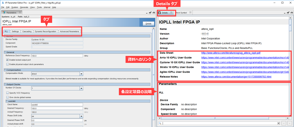
各タブ内の主な設定項目について概要を説明します。
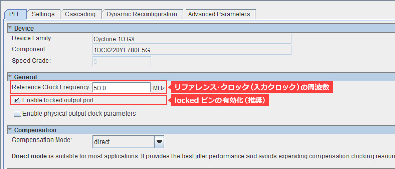
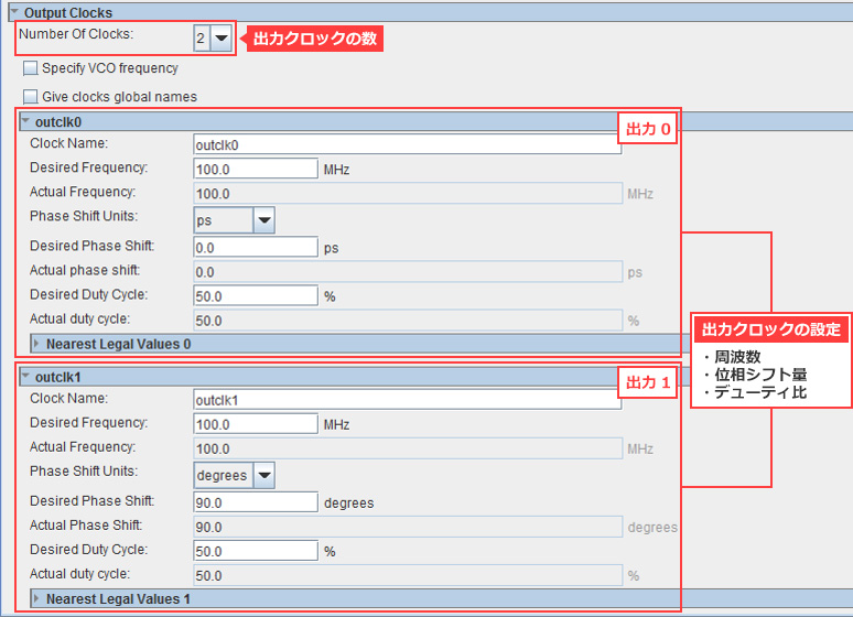
PLL タブ
リファレンスクロック(入力クロック)の周波数や locked ピンの有効/無効、出力クロックの数、出力クロックの設定などの一般的な設定を行います。
ここでは一例として、下表のように設定することにします。
| Reference Clock Frequency |
50 (MHz) |
| Enable locked output port |
✔ (On) |
| Compensation Mode |
direct |
| Number Of Clocks |
2 |
|
outclk0 |
|
| Desired Frequency |
100 (MHz) |
| Desired Pahse Shift |
0 (ps) |
| Desired Duty Cycle |
50 (%) |
|
outclk1 |
|
| Desired Frequency |
100 (MHz) |
| Desired Pahse Shift |
90 (degrees) |
| Desired Duty Cycle |
50 (%) |
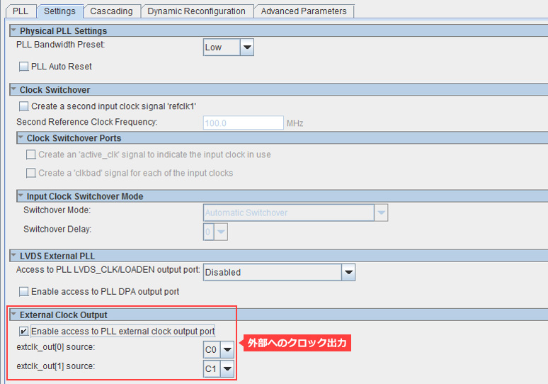
Settings タブ
PLL バンド幅プリセットや Clock Switchover(2入力を切り替える機能)、LVDS External PLL、外部クロック出力の設定を行います。
PLL で生成したクロックを FPGA 外部へ出力するには、専用ポートからの出力が推奨です。そのための設定を行います。
その他のタブは、以下のパラメーターを設定できます。詳細は、IOPLL のユーザーガイドをご覧ください。
Cascading タブ
FPGA のシリーズによっては PLL のカスケード接続をサポートしており、その設定を行います。
Dynamic Reconfiguration タブ
ダイナミック・リコンフィグレーションの設定を行います。
Advanced Parameters タブ
PLL の M/N/C カウンターの値や VCO 周波数など、PLL のパラメーター名とパラメーター値を確認できます。
各種パラメーターの設定を終えたら、IP Parameter Editor Pro の File メニュー ⇒ Save で設定内容を保存します。
右下の Generate HDL をクリックし、生成する HDL 言語の選択画面が表示されます。
Synthesis セクションでは、Quartus Prime で論理合成に使用するファイルの言語を選択します。
Simulation セクションでは、EDA シミュレーター向けのシミュレーションモデルの言語を選択します。
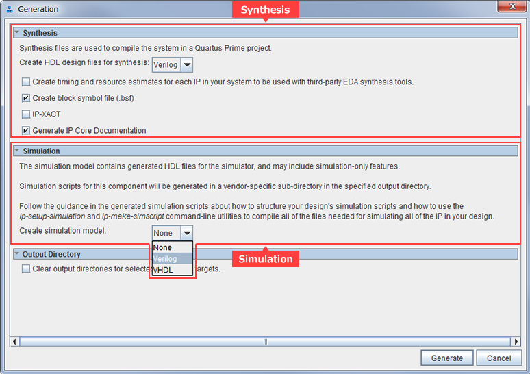
Generate をクリックし、IP を生成します。
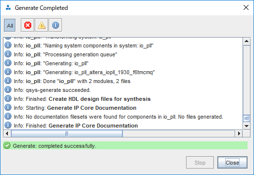
IP Parameter Editor を閉じます。
これで、IOPLL の生成が完了しました。みなさんが設計中のユーザー回路と接続して、論理設計を進めましょう。
もし、IOPLL のパラメーター設定を変更する場合は、こちらの FAQ をご覧ください。
【FAQ】 IP 編集画面の起動方法
必要な個所を編集したら、再度 IOPLL を生成してください。
2. ユーザー回路との接続
IOPLL が生成できたら、ユーザーロジックと接続します。
Verilog-HDL や VHDL に慣れていない方は、こちらを参考にしてください。このページ内の下位モジュール(ブロック)の呼び出しをご覧ください。
はじめてみよう!Verilog-HDL <演習問題つき>
はじめてみよう!VHDL <演習問題つき>
スケマティック (回路図) で設計している方は、そのままシミュレーションができませんので、HDL で設計することをお勧めします。
(※ Pro Edition には、スケマティック・ファイルを HDL に変換する機能がありません。)
3. シミュレーションで確認
それでは、シミュレーションで動作を確認してみましょう。
今回は ModelSim® - Altera® FPGA Edition を使用します。
シミュレーションで確認するにはテストベンチが必要ですが、テストベンチはユーザーが作成します。
テストベンチの作成方法については、こちらをご覧ください。
はじめてみよう!テストベンチ
テストベンチができたら、シミュレーションする準備ができました!
ModelSim® を手動で操作し シミュレーションすることもできますが、ここでは便利な方法を紹介します。参考にしてください。
msel_setup.tcl を使用したシミュレーション
おすすめ記事/資料はこちら
PLL の分周 / 逓倍(ていばい)
PLL の応用(スペクトラム拡散で EMI を減らそう!)
PLL のループ帯域幅とスペクトラム拡散のビミョーな関係
PLL
IP 関連の記事や資料 一覧
Altera® FPGA の開発フロー / トップページ