- Semiconductor BusinessHOME
- Products and Services of Macnica,Inc.
-
technical information

-
Events and Seminars
- Handling Manufacturer
- Support
- Inquiry
- Click here to purchase products
- Semiconductor business e-mail magazine registration
![]()
![]() Narrow down by specifying conditions
Narrow down by specifying conditions
現在2153件がヒットしています。check


hello.
My name is Intel F. Hanako and I provide technical support for Intel® FPGA products at Macnica.
Did you know that there are ways to debug Intel FPGAs other than using an oscilloscope or logic analyzer?
It's Signal Tap!!
* SignalTap® II was renamed to Signal Tap from Quartus Prime 17.1.


The official name is Signal Tap Logic Analyzer.
Simply put, it is a logic analyzer function of Quartus® Prime that monitors the internal signals of a user circuit implemented in an FPGA.
Its features are
- Implement Signal Tap IP in logic elements (LEs) and free memory space inside the FPGA
- View Observation Data on the Quartus® Prime Screen
- The board and Quartus® Prime communicate via a download cable used for programming, such as the Intel® FPGA Download Cable II.
- The monitor pin for the observation signal uses the JTAG pin of the FPGA.
- No need to reserve user I/O pins for debugging!
- External devices such as logic analyzers and oscilloscopes are not required!
- Free to use!
let's prepare
These are required to run the Signal Tap logic analyzer on your FPGA.
|
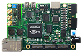
Board with FPGA |
Target Device Intel® Agilex series / Stratix® series / Arria® series / Cyclone® series / MAX® 10
|
|
development software |
Quartus® Prime Pro Edition / Quartus® Standard Edition / Quartus® Lite Edition
|
|
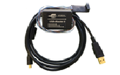
download cable |
Intel® FPGA Download Cable II (formerly USB-Blaster™ II)
|

what kind of work do you do
Work in just 4 steps!
In addition, the user design for which Signal Tap is to be implemented must have logic synthesis or placement and routing completed in advance.
Let's try it
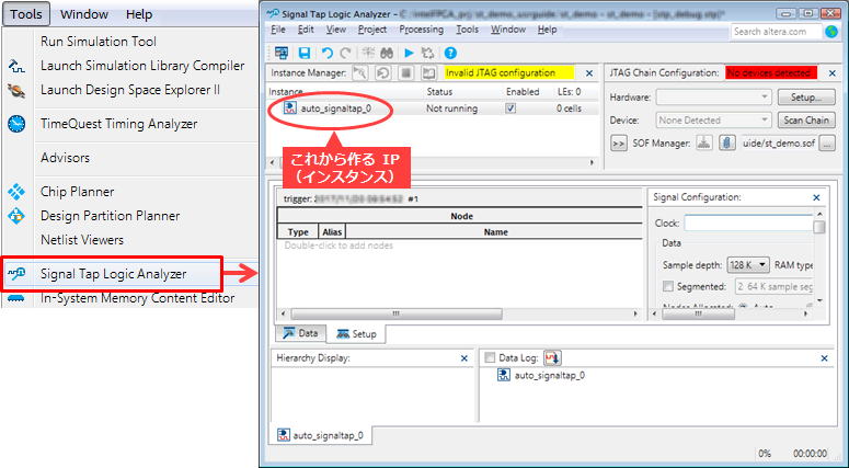
1. Create SignalTap IP
Create a new STP file. By setting the conditions on this sheet, you can create an IP.
- Specify sampling clock
In the Signal Configuration window, select the clock from your circuit that the Signal Tap will use to operate.
Signal Tap samples the monitor signal on the rising edge.
As with a normal logic analyzer, the accuracy of the monitor signal depends on the frequency of the sampling clock.
It is also possible to supply a separate clock from outside the FPGA.
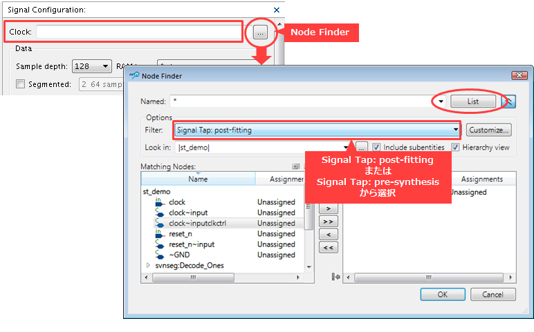
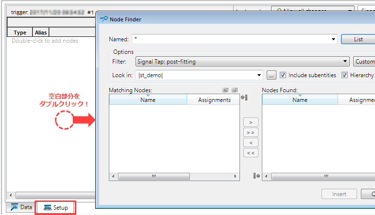
Please refer to the following document for how to use Node Finder. (Search for "Node Finder" as a keyword.)
Quartus® Prime - Constraint Method (Assignment Editor)
- Select the monitor signal
Use NodeFinder to select the signal to be monitored. The selected signal can also be used as a trigger condition. However, the signal specified as the sampling clock cannot be monitored.
Hanako's little points ♪
When registering the internal signals you want to observe in an STP file, there is a way to do so without using the Node Finder.
That's using Technology Map Viewer!
You can visually select the signal and register it with a click. This is the method I recommend.
For more information, please see this article.
How to easily register internal signals you want to capture with Signal Tap in an STP file
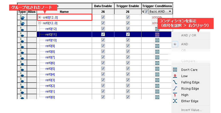
- Set the trigger condition
Select the condition for the signal you want to use as the trigger condition.
2. Implement and compile the Signal Tap IP in your design.
On the STP file, select File menu > Save As and name the STP file.
The message "Do you want to enable Signal Tap File "file name.stp" for the current project?" will be displayed. Select Yes to register it to the project. (See the confirmation method below.)
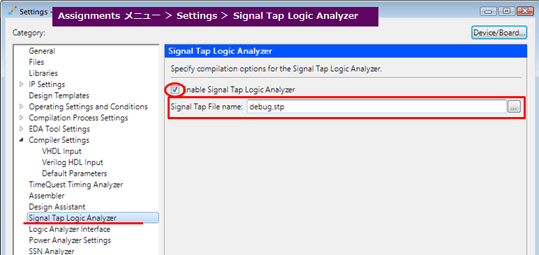
This completes the implementation of Signal Tap! There is no need to write any code to connect it.
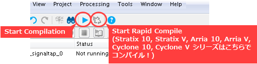
Then, click the icon on the STP file to compile the user design that contains the Signal Tap IP.
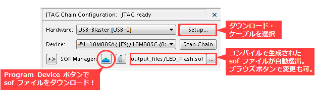
3. Download the .sof to the FPGA
Select the download cable in the JTAG Chain Configuration window in the STP file (top right) and confirm the sof file to transfer. Then click the Program Device button to start downloading!
4. Acquisition and observation of sampling data
Clicking the Run Analysis button will display the STP file with the most recent sampling data that hit the trigger event.
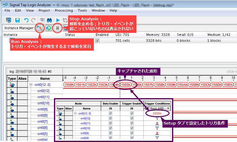
If you just change the High or Low trigger condition, there is no need to recompile.
After changing the value, simply click the Run Analysis button immediately.
See, it's easy ♪
If you just want to quickly observe the internal signals of your FPGA, you can easily debug with Signal Tap without having to pull out large equipment such as a logic analyzer.
Hanako's little points ♪
Recompiling after implementing Signal Tap IP has the disadvantage of increasing compilation time and affecting layout, but by using the incremental compilation feature of Quartus® Prime, users can reduce this stress. (The Lite Edition does not support incremental compilation, so it cannot be used with the Lite Edition.)
Also, if you make changes during debugging that affect the circuit configuration of the Signal Tap IP, such as adding/removing a Signal Tap instance, adding/removing a signal to be sampled or a signal used for a trigger condition, or changing the sampling clock, you will need to compile again.
For more information, please see the document below.
Design Debugging with the Signal Tap Logic Analyzer (Quartus Prime Standard Edition)
Design Debugging with the Signal Tap Logic Analyzer (Quartus Prime Pro Edition)
At the end
This time we introduced the Signal Tap logic analyzer.
Are you eager to try out the Signal Tap logic analyzer function?
Using the following tutorials, sample designs, and corresponding evaluation and development kits, you can easily experience the work flow from creating Signal Tap IP to debugging on a real device.
◆ Tutorial: Document
quartus_signaltap_tutorial_v1710_r1__1.pdf
◆ Tutorial: Sample Design for Cyclone® 10 LP FPGA Evaluation Kit
◆ Tutorial: Sample Design for MAX® 10 FPGA Evaluation Kit
◆ Tutorial: Design-only project

To use SignalTap® II (now Signal Tap) in Quartus® Prime Lite Edition 16.0 and earlier versions, a "spell" is required.
The magic spell is to"enablethe TalkBack function"!
Follow the steps below to enable the TalkBack feature:
- Select Tools menu ⇒ Options
- Select Internet Connectivity from Category in the Options window
- In the Internet Connectivity dialog window, click the TalkBack Options button
- In the TalkBack Options window, check the Enable sending TalkBack data to Altera option.
That's it!
[Related FAQ] What is the TalkBack feature?
Click here for recommended articles/materials
Quartus® Getting Started Guide - Using the Signal Tap Logic Analyzer
List of FAQs about Signal Tap (formerly SignalTap® II)
Click here to purchase products
Intel® FPGA Download Cable II (formerly USB-Blaster™ II)
Intel® FPGA Download Cable (formerly USB-Blaster™)
Intel® FPGA Ethernet Cable II (formerly EthernetBlaster™ II)