- Semiconductor BusinessHOME
- Products and Services of Macnica,Inc.
-
technical information

-
Events and Seminars
- Handling Manufacturer
- Support
- Inquiry
- Click here to purchase products
- Semiconductor business e-mail magazine registration
![]()
![]() Narrow down by specifying conditions
Narrow down by specifying conditions
現在2183件がヒットしています。check
Intel® FPGAs can implement JESD204B interfaces by using the JESD204B IP core. This article describes a series of steps from generating a JESD204B loopback sample design using the Intel® Quartus® Prime software to verifying its operation on the Arria® 10 GX FPGA development kit.
More information on JESD204B interfaces in Intel FPGAs can be found here.
Intel® FPGA JESD204B IP (Intel)
This article was created with reference to the following materials, so please refer to them as well.
Arria 10 JESD204B IP Core Example Design User Guide (Intel)
JESD204B IP Core User's Guide (Intel)
environment
- Tools: Intel® Quartus® Prime Software v17.0
- Development Kit: Intel® Arria® 10 GX FPGA Development Kit < Macnica-Mouser Purchase Site >
procedure
- Create a sample design
- Confirmation of design configuration
- operation check
- Summary
- Reference information
1. Create a sample design
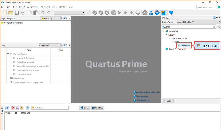
First, launch Quartus® Prime, set Device Family to Arria 10 from IP Catalog, and type JESD in the search Box.
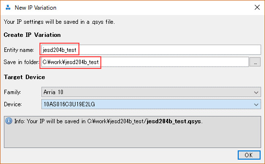
Double-click JESD204B to launch Qsys. New IP Variation will be displayed, so enter the Entity Name appropriately. Here, I called it jesd204b_test. Also, for Save in folder, specify the folder where you want to generate the example design. In this case c:\work\jesd204b_test.
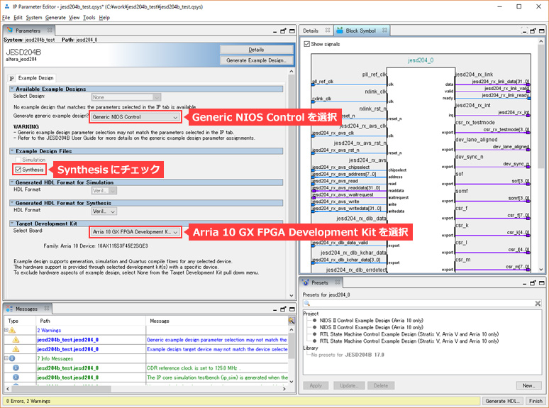
Click the OK button to save the Qsys file. The Qsys screen looks like this: Since we are going to generate an example design, select the Example Design tab. In order to check the operation on the actual machine, set the following three items and click the Generate Example Design button at the top of the screen. (Not Generate HDL on the bottom right.)
- Generate generic example design? ⇒ Select Generic NIOS Control
- Check Example Design Files ⇒ Synthesis
- Select Board ⇒ Arria 10 GX FPGA Development Kit
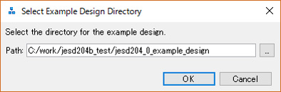
You will be prompted for a location to save the file, so specify the folder where you want to save the file and click the OK button.
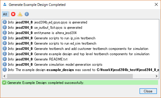
A sample design is generated.
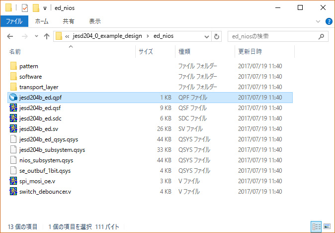
The contents of the generated ed_nios folder are as follows.
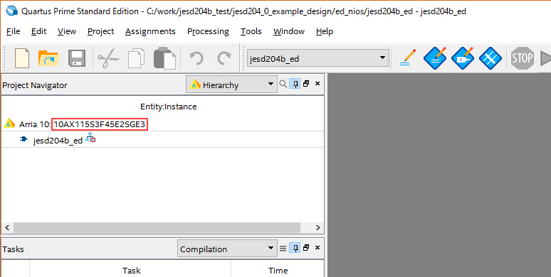
From the Quartus® Prime File menu ⇒ Open Project, select jesd204b_ed.qpf to open the generated project. Arria® 10 GX Development Kit devices are preconfigured. In Quartus® Prime v17.0, the model number is ES3 product, but it is SOF compatible with the production product, so you can proceed as is or manually change it to the production product model number. For now, let's just keep going.
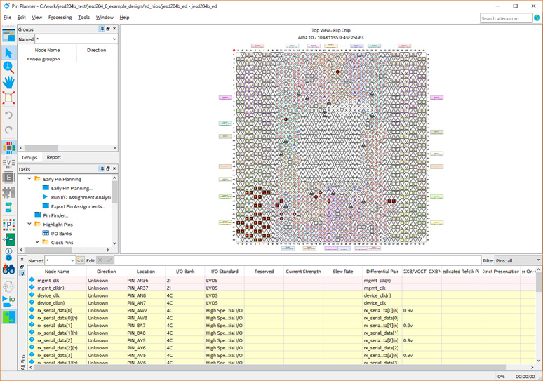
If you open the Quartus® Prime Pin Planner, you will see that the necessary pin assignments have already been made.
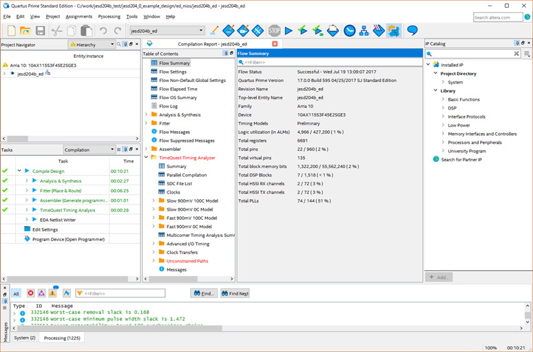
Compile the design. Execute Start Compilation in the Processing menu. When the compilation is complete, it will look like this:
2. Confirmation of design configuration
The configuration of the automatically generated sample design is as follows.
- Number of lanes (L): 2 lanes
- Number of converters in converter device (M): 2
- Number of octets in one frame (F): 2
- Lane rate: 6.144Gbps/Lane
- Device Clock: 153.6MHz
- Nios II base design
- Serial loopback within FPGA device or external loopback on FMC port A
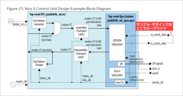
Below is the block diagram of the sample design. Since this sample design is for verification of JESD204B IP core in FPGA, it is possible to send and receive PRBS data by serial loopback in FPGA device or external loopback on FMC port A. It's purpose is to make sure you're communicating. The Nios II software performs processing such as initialization of each component in the device, control of the Test Pattern Generator/Checker, and sending of sysref.
For more information, refer to the Arria 10 JESD204B IP Core Example Design User Guide.
3. Operation check
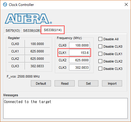
First, configure the hardware. Connect the JTAG and power cables to your Arria® 10 FPGA Development Kit and power it on. Execute ClockControl.exe that comes with the kit and set CLK1 of SI5338 (U14) to 153.6MHz.
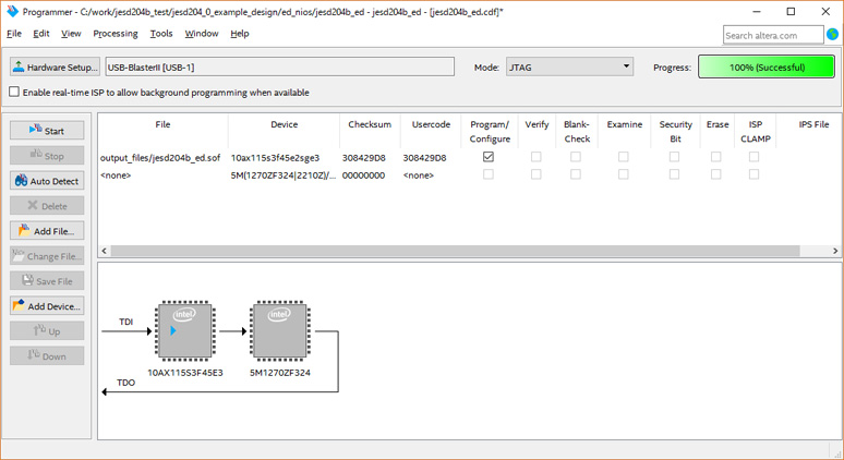
Start Programmer and write SOF file.
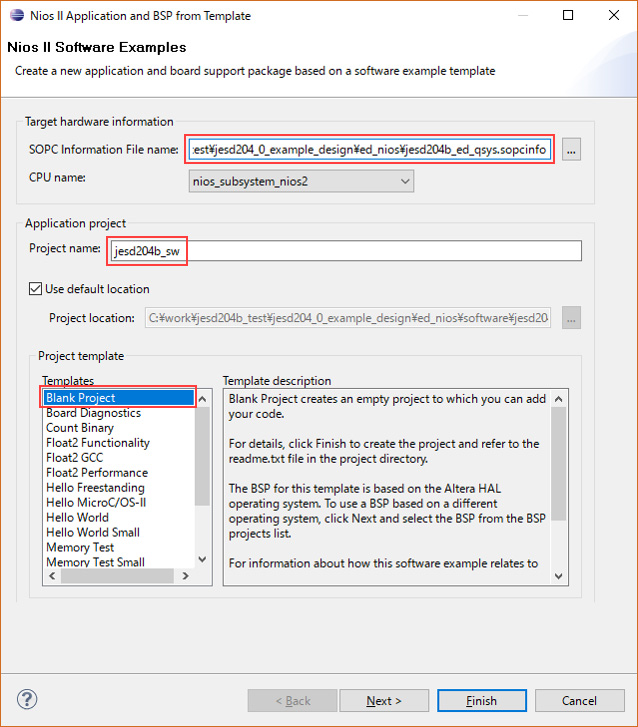
Create software for Nios® II using the C language source code in the software folder. Start the Nios® II software Build Tools for Eclipse (Nios® II SBT hereafter) and configure as follows. The project name is arbitrary, but enter jesd204b_sw here. Click Finish to create the software project.
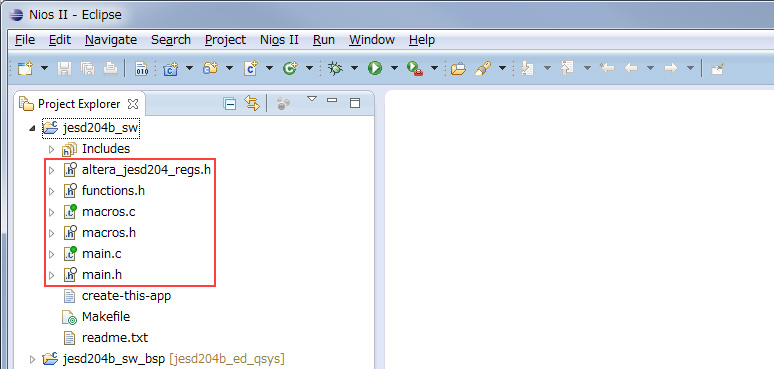
Import the source files in the source folder into the Nios® II SBT.
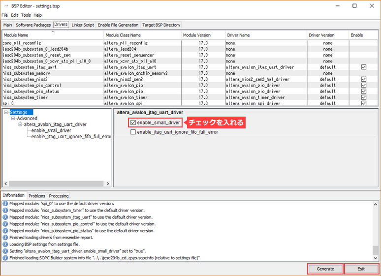
Launch the BSP Editor (right click on the jesd204b_sw_bsp project ⇒ Nios II ⇒ BSP Editor). Check enable_small_driver for altera_avalon_jtag_uart_driver in the Drivers tab. This setting ignores the interrupt signal from the JTAG UART and operates. After setting, click the Generate button, then the Exit button to close the BSP Editor.
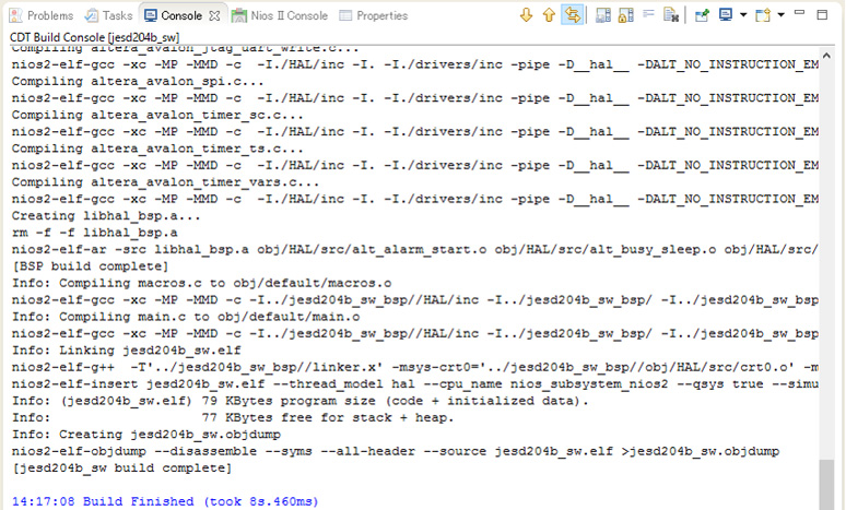
Build the software (right click on the jesd204b_sw project ⇒ Build Project). A successful completion looks like this:
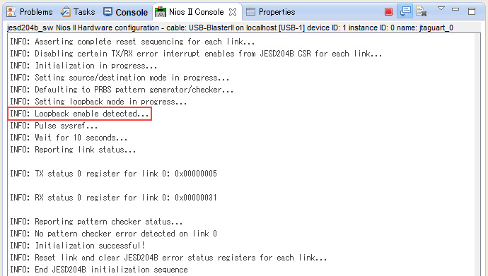
Run the Nios® II software (right click on the jesd204b_sw project ⇒ Run As ⇒ Nios II Hardware). On successful execution, you will see the execution log in the Nios II Console as shown below.
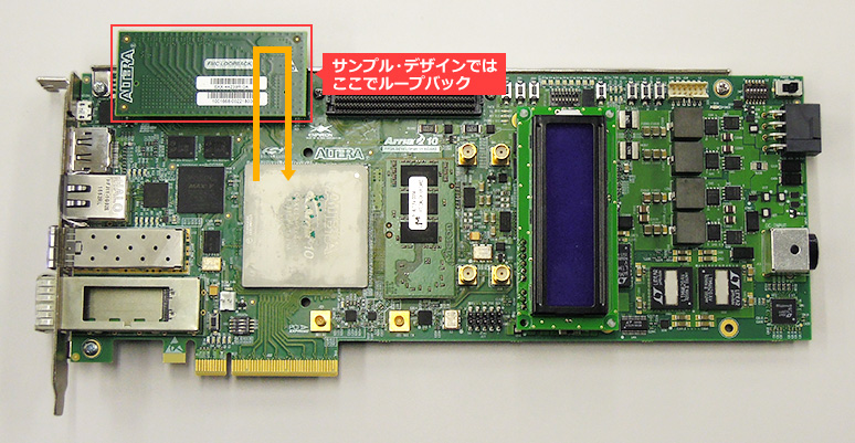
The initial state of the software is a serial loopback setup within the FPGA device. With a software configuration change, FMC port A can be configured for external loopback. Implement the FMC Loopback connector attached to FMC port A as follows:
Edit main.h as follows and rebuild the Nios® II software. Once the rebuild is complete, run the Nios® II software (right click on the jesd204b_sw project ⇒ Run As ⇒ Nios II Hardware).
before editing
#define LOOPBACK_INIT 1
After editing
#define LOOPBACK_INIT 0
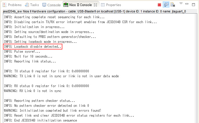
Looking at the log after execution, you can confirm that the message regarding Loopback is as follows.
INFO: Loopback disable detected...
By the way, in case of serial loopback inside FPGA device, it will be displayed as below
INFO: Loopback enable detected...
4. Summary
With the work up to this point, we were able to confirm high-speed serial communication with the JESD204B IP core mounted in the FPGA. The next step is to establish communication by mounting the evaluation board for the DA converter (transmitting side as seen from the FPGA) or AD converter (receiving side as seen from the FPGA) to be used. In short, the following implementations are required:
- Clock-related connections (Device Clock, sysref, sync_n, etc.)
Since the specifications differ depending on the AD/DA converter evaluation board used, it is necessary to understand the details before implementing.
- Implementing register settings in DA/AD converter devices using interfaces such as SPI
In the design I introduced, the SPI interface is implemented as standard, so if the AD/DA converter evaluation board to be used supports SPI, you can make the wiring correctly and implement the control part from the software. It can be easily realized.
Also, from the following page introduced at the beginning, you can download the reference design that was actually tested by Intel, so please refer to it as a reference for implementation.
Intel® FPGA JESD204B IP Page
5. Reference information
For Intel® FPGA, we actually conducted communication tests with several representative AD/DA evaluation boards and published them in the form of checkout reports. The following are relatively new releases.
AN 710: Altera JESD204B MegaCore Function and ADI AD9680 Hardware Checkout Report
AN 712: Altera JESD204B MegaCore Function and ADI AD9625 Hardware Checkout Report
AN 719: Altera JESD204B IP Core and TI DAC37J84 Hardware Checkout Report
AN 733: Altera JESD204B IP Core and TI ADC12J4000 Hardware Checkout Report
AN 749: Altera JESD204B IP Core and ADI AD9144 Hardware Checkout Report
AN 753: Altera JESD204B IP Core and ADI AD6676 Hardware Checkout Report
AN 779: Altera JESD204B IP Core and ADI AD9691 Hardware Checkout Report
AN 810: Intel JESD204B IP Core and ADI AD9208 Hardware Checkout Report
AN-785: Altera JESD204B IP Core and ADI AD9162 Hardware Checkout Report
AN-792: Intel JESD204B IP Core and ADI AD9371 Hardware Checkout Report
Click here for recommended articles/materials
Click here for IP-related articles and resources...