- Semiconductor BusinessHOME
- Products and Services of Macnica,Inc.
-
technical information

-
Events and Seminars
- Handling Manufacturer
- Support
- Inquiry
- Click here to purchase products
- Semiconductor business e-mail magazine registration
![]()
![]() Narrow down by specifying conditions
Narrow down by specifying conditions
現在2189件がヒットしています。check
This article provides a simple explanation of the process of implementing a DDR3 SDRAM memory controller in an Altera® FPGA and simulating and verifying operation using an example design. This page uses the Beryll Cyclone V GX basic board (Beryll board) with a Cyclone® V device implemented, but the basic flow is the same for Stratix® series and Arria® series devices that support UniPHY-based DDR3 SDRAM controllers.
<Agenda>
1. Check DDR3 SDRAM Support in Cyclone® V Devices
The support status of the DDR3 SDRAM interface can be checked using the External Memory Interface Spec Estimator, as introduced in "Implementing an External Memory Controller in an Altera® FPGA! (Preparation)".
We will enter conditions into the External Memory Interface Spec Estimator. Click the "Decide Search Conditions and Items" button and enter the following conditions, such as the Cyclone® V device (model number: 5CGXFC4C6F27C7N) implemented on the Beryll Cyclone V GX Basic Board (Beryll board) used in this test, memory, and board specifications.
- Family: Cyclone® V GX
- Temperature Range & Speed Grade: Commercial Temperature Range (C), -7
- Interface type: soft, hard
- Memory standard: DDR3
- Memory Topology & Rank: Component, 1 Chip Select
The search results are as follows. By the way, the C7 in the second half of the model number represents the temperature range and speed grade.
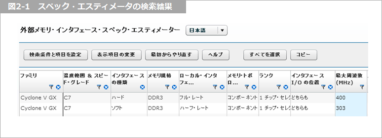
From this search result, we can confirm on the Beryll board that
- With a hard memory controller (HMC), the maximum frequency is 400 MHz (800 Mbps)
- With Soft Memory Controller (SMC), the maximum frequency is 303 MHz (606 Mbps)
That's what it means. So this time
- Hard Memory Controller (HMC) with memory interface frequency of 400 MHz (800 Mbps)
I would like to move it with
Now let's generate a controller using the Altera® Quartus® Prime software!
<Tools to be used>
- Quartus® Prime Development Software v16.0: Standard Edition or Lite Edition
- Standard Edition: Paid license required
- Lite Edition: No license required
- ModelSim® - Altera® FPGA Edition 10.4d (Quartus® Prime 16.0)
- ModelSim® - Altera® FPGA Edition: Paid license required
- ModelSim® - Altera® FPGA Starter Edition: No license required
Have you installed the tool?
If you haven't installed it yet, you can get it from the Altera® FPGA website (download).
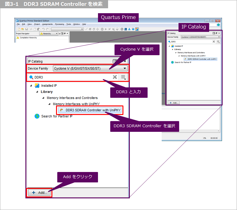
2. Generating a DDR3 SDRAM Controller with UniPHY
First, let's generate the memory controller!
Launch the Quartus® Prime software and search for DDR3 SDRAM Controller with UniPHY by entering DDR3 in the IP Catalog search bar.
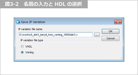
A screen will appear where you can set the directory in which various controller-related files will be generated and the name of the controller. Also select the generation language (Verilog or VHDL) and click OK. At this time, avoid using full-width characters or half-width spaces in the path or file name! In this example, we will name the controller ddr3.
This will bring up the controller settings screen. Let's make the necessary settings!
First, enable the HMC.
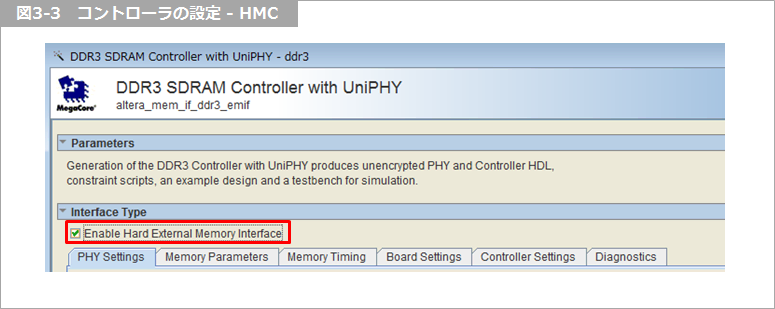
From here on, we will make the necessary settings, but this time we will only make the minimum settings necessary to check operation on the Beryll board. We will leave everything else as default.
For more information, see the EMIF Handbook.
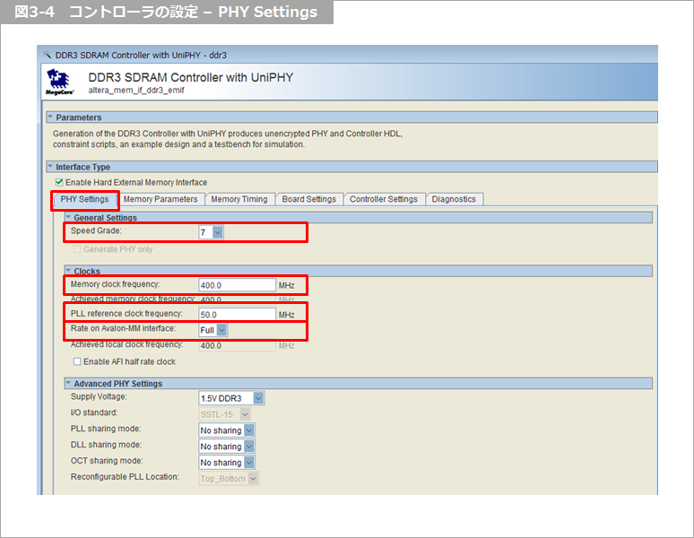
PHY Settings tab
This time, we will use a 50 MHz clock as the reference clock. In the PHY Settings tab, make the following settings:
- Speed Grade: 7
- Memory clock frequency: 400.0MHz
- PLL reference clock frequency: 50.0MHz
- Rate on Avalon-MM interface: Full
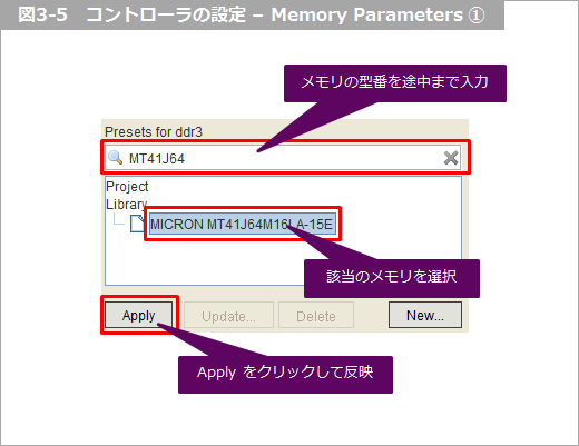
Memory Parameters tab
The DDR3 SDRAM on the Beryll board is two Micron MT41J64M16s, each 16-bit wide, for a total of 32-bits wide.
Search for an installed memory from Preset for... on the right. Typical memories are pre-listed here, with detailed parameters already set. Luckily, an installed memory was available, so select it and click Apply. This will update the memory's configuration and parameters. If the memory you want to use is not on the list, select a memory with a similar configuration, edit the parameters while looking at the datasheet, give it a name, and save it for easy recall in the future.
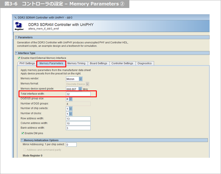
On the Beryll board, data is connected between the Cyclone V device and memory at a 32-bit width, so I will also perform this verification at a 32-bit width.
This time, only the following settings will be configured in the Memory Parameters tab.
- Total interface width: 32
Memory Timing tab
Since the memory information was reflected on the Memory Parameters tab earlier, leave the settings as they are.
Board Settings tab
For now, leave the defaults.
Controller Settings tab
For now, leave the defaults.
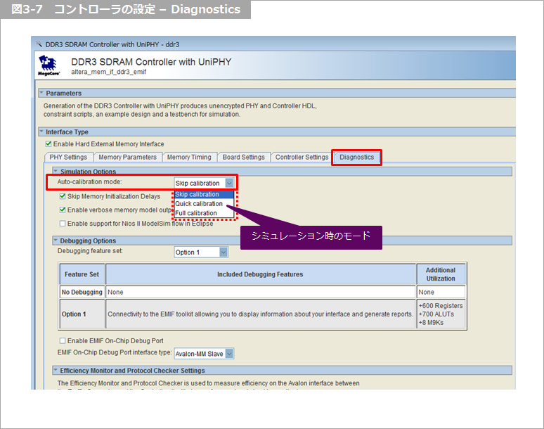
Diagnostics tab
This time, we will only set Auto-calibration mode. This setting is only valid for simulation and does not affect the operation of the actual device.
The DDR3 SDRAM interface cannot be read/written immediately after power-on; it must first be initialized and calibrated. We won't go into detail here, but unless these steps are taken, you won't be able to access it, such as read/write.
This calibration can be skipped in the simulation. Of course, you can check the full calibration behavior in the simulation, but depending on the configuration, it may take a considerable amount of time, so be prepared. The Auto-calibration mode sets the degree to which this calibration is omitted.
- Skip calibration: skip calibration
- Quick calibration: perform a partial calibration
- Full calibration: Execute without skipping calibration
Generating the Controller
Click Finish to generate the controller. At this time, if you check Generate Example Design as shown below and click Generate, an environment (Example Design) will also be generated at the same time, allowing you to easily perform simulations and run the controller on a real device.
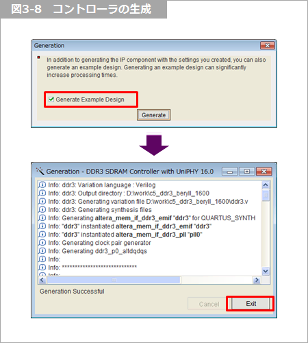
Generating the controller will take a few minutes. Once it is complete, click Exit.
For more information, please see "Running DDR3 on Altera® FPGA! (Practical Edition) [2/2]".
Manufacturer information
External Memory Interface (Altera® site)
Click here for recommended articles/materials
EMIF Design & Debug Guidelines for FPGAs
Implementing an external memory controller in an Altera® FPGA!
Altera® FPGA Development Flow / Top Page