- Semiconductor BusinessHOME
- Products and Services of Macnica,Inc.
-
technical information

-
Events and Seminars
- Handling Manufacturer
- Support
- Inquiry
- Click here to purchase products
- Semiconductor business e-mail magazine registration
![]()
![]() Narrow down by specifying conditions
Narrow down by specifying conditions
現在2189件がヒットしています。check
This page aims to provide a simple explanation of the process of implementing a DDR4 SDRAM memory controller in an Altera® FPGA, simulating it using an example design, and verifying its operation. This page focuses on the Arria® 10 GX FPGA Development Kit, which is equipped with an Arria® 10. However, the basic flow is the same for other FPGAs that support a DDR4 SDRAM controller.
environment
- Development Tools: Altera® Quartus® Prime Design Software v17.1 (Pro Edition or Standard Edition)
- Pro Edition: Paid license required
- Standard Edition: Paid license required
- Simulation tool: ModelSim® - Altera® FPGA Edition 10.5b (Quartus® Prime 17.1)
- ModelSim® - Altera® FPGA Edition: Paid license required
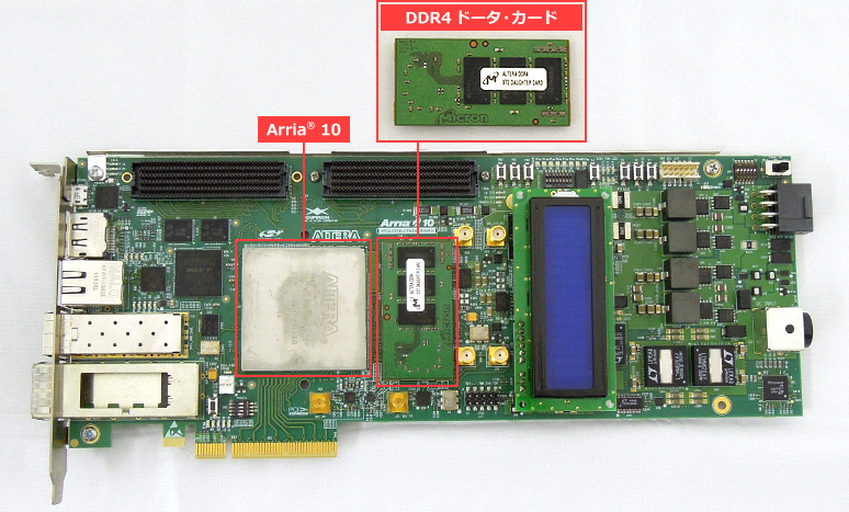
- Development Kit: Altera® Arria® 10 GX FPGA Development KitMacnica -Mouser Purchase Site
Compare Quartus® Prime Editions
Have you installed the tool?
If you haven't installed it yet, you can get it from the Altera® FPGA website (download).
procedure
- Checking DDR4 SDRAM interface support
- DDR4 SDRAM Controller IP Settings
- Running a functional simulation
- Compiling the Example Design
- Actual machine operation check
1. Check whether the DDR4 SDRAM interface is supported
For the support status of the DDR4 SDRAM interface, please refer to Implementing an external memory controller in an Altera® FPGA! As introduced in ", External Memory Interface Spec Estimator You can check it out at:
We will input the conditions into the external memory interface spec estimator. Altera® Arria® 10 GX FPGA Development Kit Click the "Determine search conditions and items" button and enter the following conditions, such as the Arria® 10 (model number: 10AX115S2F45I1SG) implemented in the board, memory, and board specifications.
- Family: Arria® 10 GX and GT
- Temperature Range & Speed Grade: Industrial Temperature Range (I), -1
- Interface type: Hard
- Memory standard: DDR4
- Memory Topology & Rank: Component, UDIMM
The search results are as follows. The I1 in the last part of the part number indicates the temperature range & speed grade.
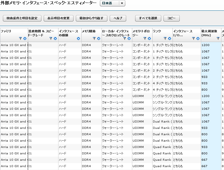
From these results, you can see that even for components (memory devices), the upper limit of the maximum memory interface frequency differs depending on whether the chip select is 1, 2, or 4. Also, even for UDIMM (Unbuffered DIMM), the upper limit of the maximum frequency differs depending on whether it is single rank or dual rank.
Now let's generate a controller using the Altera® Quartus® Prime software!
2. Configuring the DDR4 SDRAM Controller IP
You can easily search for Arria® 10 External Memory Interfaces by launching Quartus® Prime and entering "Arria® 10 External..." in the IP Catalog search bar. (The Standard Edition of Quartus® Prime can be used without a project open, but the Pro Edition cannot be used without a project open.)
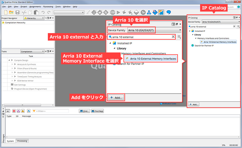
Click Add to launch the IP Parameter Editor and open a screen to enter the name and target device. Here: The target device is the device implemented in the Arria® 10 GX FPGA development kit.
- Entity name: ddr4
- Save in folder: C:\Work\a10_ddr4_1710
- Family: Arria® 10
- Device: 10AX115S2F45I1SG
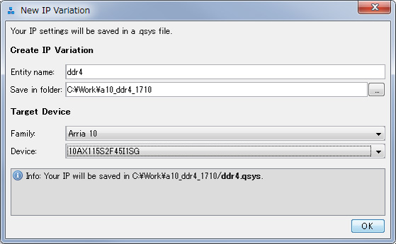
Click OK to display the IP Parameter Editor. Let's make the necessary settings!
Parameters in the center is an area where various necessary settings are made, and Details on the upper right has links to documents and descriptions of each setting item.
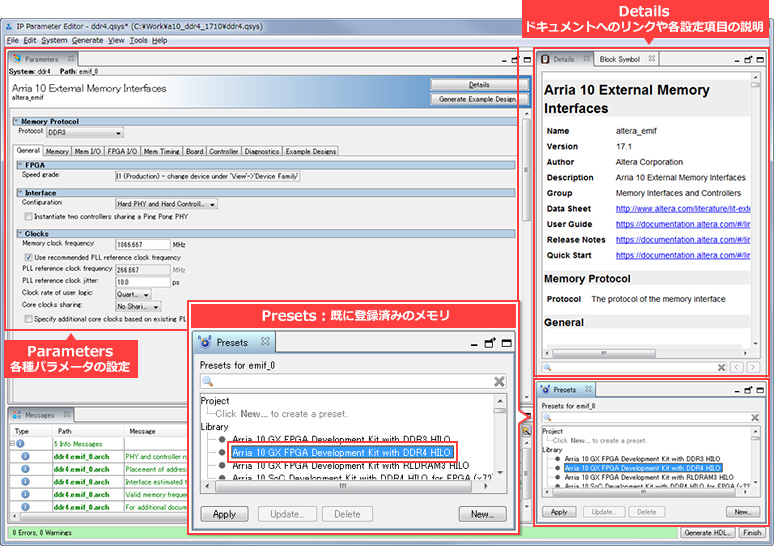
The Presets menu contains a selection of popular memory options. To test the Arria® 10 GX FPGA Development Kit, select the DDR4 daughter card included with the kit (Arria® 10 GX FPGA Development Kit with DDR4 HILO). Click Apply. This automatically applies most of the memory parameter settings.
Now, let's configure the settings required for this operation check on each tab in Parameters. Leave the other settings as default. For detailed explanations of each setting, please refer to the Details mentioned earlier.
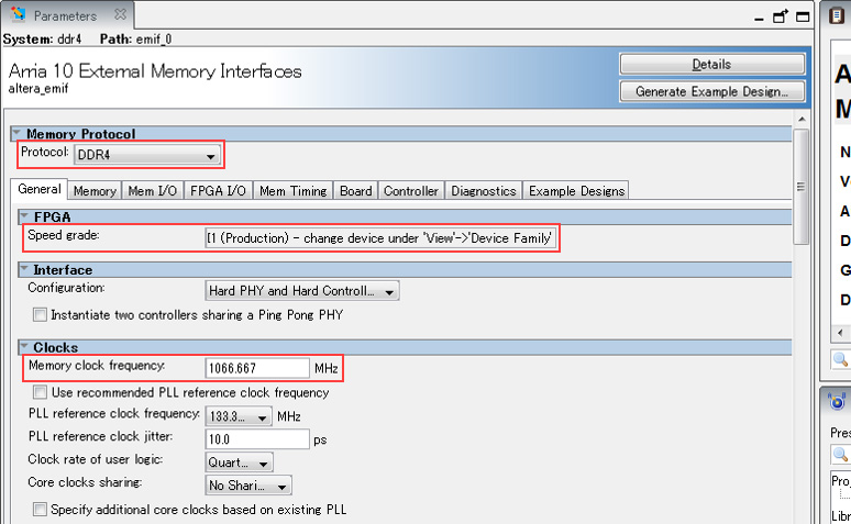
General tab
Make sure that Protocol is set to DDR4. This should be automatically reflected in the Presets mentioned earlier.
Next, make sure that the Speed Grade (FPGA speed grade) is set to I1. This should be automatically reflected when you select the target device along with the controller name.
Leave the other settings as default. By the way, the memory interface frequency is 1066.667MHz.
Memory tab
Leave as default.
Mem I/O tab
Leave as default.
FPGA I/O tab
Leave as default.
Mem Timing tab
Leave as default.
Board tab
Leave as default.
Controller tab
Leave as default.
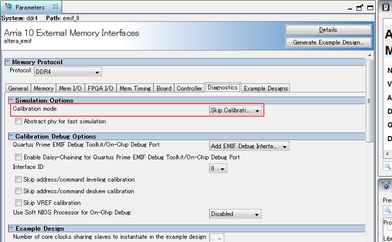
Diagnostics tab
Simulation Options - Calibration mode
This setting is only valid for simulation and does not affect the actual operation of the device.
The DDR4 SDRAM interface cannot be read/written immediately after powering on; it must first be initialized and calibrated. We won't go into detail here, but unless these steps are taken, you won't be able to access it, such as read/write.
You can skip this calibration in the simulation. Of course, you can also check the full calibration behavior in the simulation, but depending on the configuration, it may take a considerable amount of time.
- Skip calibration: skip calibration
- Full calibration: Execute without skipping calibration
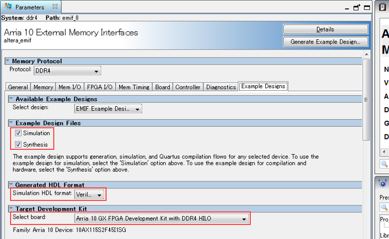
Example Designs tab
Example Design Files
- Simulation
Check this box when simulating with Example Design. - Synthesis
If you want to check the actual machine with Example Design, please check it.
Generated HDL Format - Simulation HDL format
Select the HDL to simulate.
Target Development Kit - Select board
Select the target board. However, since you configured the Arria® 10 GX FPGA Development Kit with DDR4 HILO included with the Arria® 10 GX FPGA Development Kit in the Presets section above, it should already be selected.
Save this setting when you are done. Select File menu ⇒ Save As in IP Parameter Editor and save it as ddr4.qsys here.
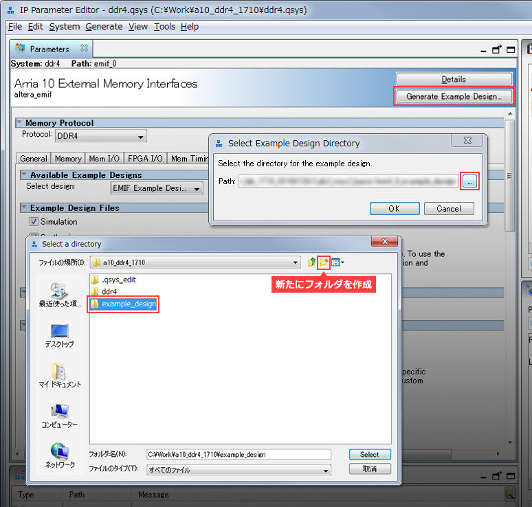
Next, generate the Example Design. Click Generate Example Design, specify where to generate the Example Design, then click Generate. This time I specified C:\Work\a10_ddr4_1710\example_design as the generation location.
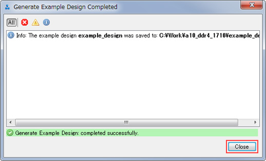
It will take a few minutes to generate the Example Design. If it can be generated successfully, the following window will be displayed, so click Close.
This time, we will check the operation using the example design, so we will not generate a controller. If you plan to implement a controller in your FPGA design, please generate a controller.
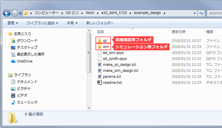
When the Example Design is generated, a qii folder, a sim folder, etc. are generated.
3. Running a functional simulation
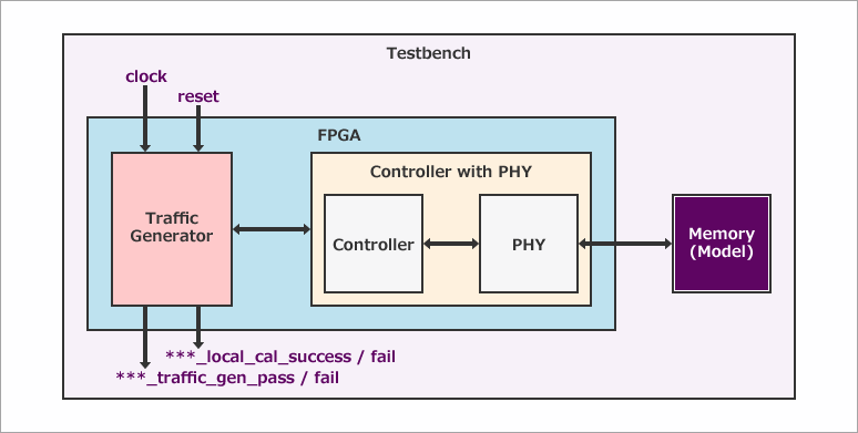
Let's try running a functional simulation. The files required to run a simulation (such as a simulation project, test bench, traffic generator, and memory model) are automatically generated when you generate the controller, so you can run the simulation without any hassle.
To briefly explain how the simulation works, the traffic generator receives a clock and sends addresses, commands, and data to the memory controller, which then writes them to the memory via the PHY. The data read from the memory is then compared with the data written. If they match, Success = High; if they do not match, Fail = High.
This time, we will use ModelSim® - Altera® FPGA Edition to simulate the design.
After launching ModelSim® - Altera® FPGA Edition, select File menu ⇒ Change Directory and specify the working directory. In this example, specify C:\Work\a10_ddr4_1710\example_design\sim\ed_sim\mentor. Since ModelSim® is a simulator from Mentor Graphics®, specify the mentor folder.
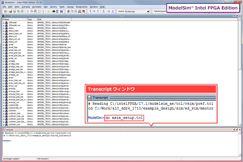
Next, execute the following commands in the Transcript window of ModelSim® - Altera® FPGA Edition in the following order:
- do msim_setup.tcl (execute script for simulation)
- ld_debug (compile libraries/compile design files/load design)
- add wave "ed_sim/*" (capture signal in wave window)
- run -all (run the simulation)
Although it depends on the PC specifications, with this configuration, it took about 30 minutes to complete the simulation using ModelSim® - Altera® FPGA Edition. (By comparison, it took about 4 minutes on Questa® Prime/Core.)
The simulation will automatically stop when it is finished. If you want to check the waveform after the simulation is complete, click No. (Note that clicking Yes will close ModelSim® - Altera® FPGA Edition.)
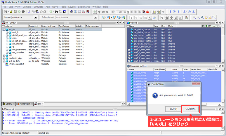
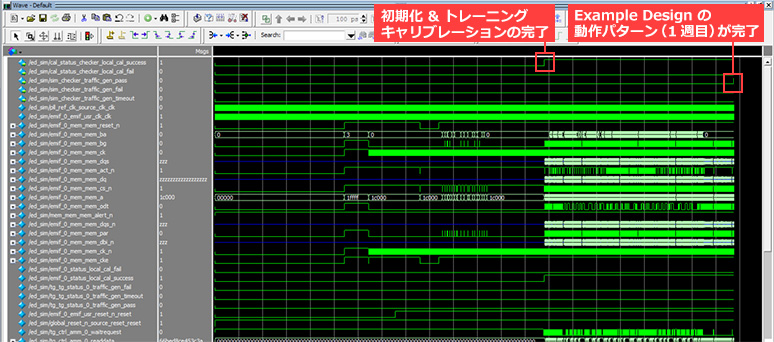
Looking at the simulation waveform, you can confirm that ***_local_cal_successis High when intermediate calibration is completed. Calibration waveforms are omitted in Skip Calibration simulations.
Also, the simulation is complete when ***_traffic_gen_pass goes High. The Example Design repeats the operation of writing/reading and comparing, but the simulation ends after the first week. However, it can be used for long-run tests because it continues for a long time in the actual machine confirmation.
4. Compiling the Example Design
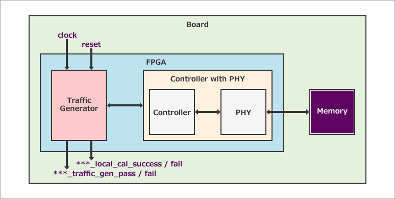
Next, prepare to compile the Example Design. Below is a block diagram of the Example Design.
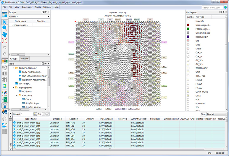
Various settings, constraints, and pin assignments are required to compile, but the Example Design generated for the Arria® 10 GX FPGA Development Kit already has various settings, constraints, and pin assignments. Just in case, let's take a look at Pin Planner. Select Assignments menu ⇒ Pin Planner in Quartus® Prime.
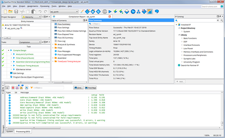
Let's actually compile. Select Quartus® Prime Processing menu ⇒ Start Compilation.
Did the compilation finish normally?
<Supplement>
The timing analysis result (TimeQuest Timing Analyzer in the compilation report) is in red. This is due to the lack of timing constraints for all pins. However, the unconstrained pins are reset, JTAG related, and LED output pins, so we will proceed as is for now.
If there is a timing violation in Setup or Hold, try changing the compile settings. Set to Performance in the Quartus® Prime Assignments menu ⇒ Settings ⇒ Compiler Settings ⇒ Optimization mode. This setting aims to compile performance-oriented, so it tends to improve timing, but there are cases where it consumes a lot of resources.
5. Operation check using development kit
Once compilation is complete, write the SOF file generated by compilation to the Arria® 10 device. Connect the development kit to your PC with a USB cable (development kit side: USB Micro-B) and turn on the power.
<Additional Information>
Altera® FPGAs have a JTAG port, through which data is written via an Altera® FPGA download cable.
While an Altera® FPGA download cable (such as USB-Blaster™ or USB-Blaster™ II) is typically used, the Arria® 10 GX FPGA Development Kit has the Blaster functionality built into the board, eliminating the need for a separate download cable; data can be written using just the USB cable.
Install the included DDR4 daughter card in the center of the development kit.
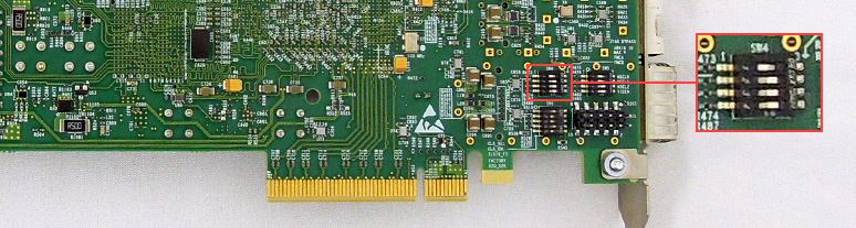
Also check the JTAG chain setting (DIP switch/SW4 on the back).
- 1: OFF (left side)
- 2: ON (right side)
- 3: ON (Right side)
- 4: ON (Right side)
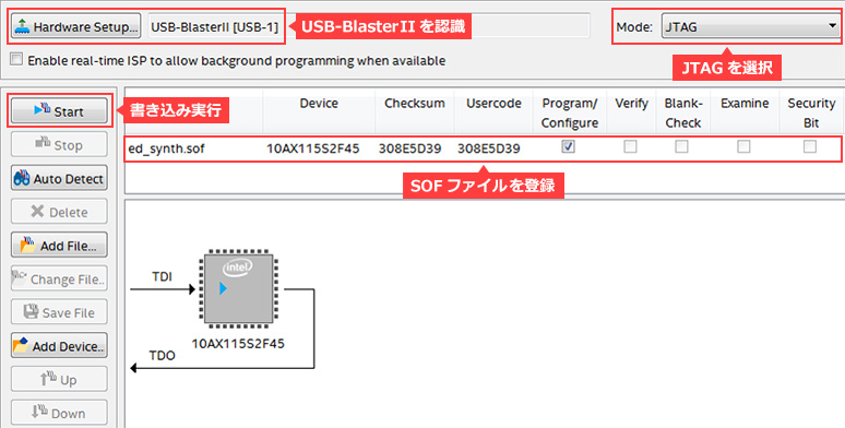
Then select Tools menu ⇒ Programmer in Quartus® Prime to launch the Quartus® Prime Programmer.
If the Programmer starts and the SOF file for writing is automatically registered, confirm that Hardware Setup and Mode are selected, then click Start to execute writing.
If the SOF file is not registered in the Programmer, set the download cable, mode, and write file as follows, then click Start to execute the write.
- Hardware Setup: USB-Blaster™ II (Cannot be selected unless the USB-Blaster™ II driver is installed) ⇒ How to install the USB-Blaster™ II driver
- Mode: JTAG
- Add File: SOF file generated during compilation (file name: ed_synth.sof)
After writing the SOF file, the Example Design actually works. In normal operation, the green LED should be on.
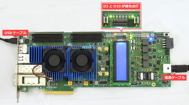
The LEDs are assigned as shown in the table below. These pin assignments are also automatically assigned in the Example Design for the development kit.
| pin name | LED | Explanation |
| ***_status_local_cal_success | D3 green | Asserted high upon successful completion of memory initialization, training, and calibration, indicating the controller is ready to use the memory interface. |
| ***_status_local_cal_fail | D3 red | Asserts high if memory initialization, training, or calibration fails. |
| ***_tg_0_traffic_gen_pass | D10 Green | When the first cycle of the memory write/read operation check pattern by the example design is completed (normally), this signal is asserted high. The simulation stops after one cycle, but the example design for operation check repeats the operation check pattern. |
| ***_tg_0_traffic_gen_fail | D10 red | Asserted to High when the first cycle of the memory write/read operation check pattern by Example Design is completed (failed). In the simulation, it stops after one round, but in the Example Design for operation confirmation, the operation confirmation pattern is repeated. |
| ***_tg_0_traffic_gen_timeout | D7 green | Asserted high when the example design's memory write/read operation check pattern times out. |
You can also use the Signal Tap logic analyzer function to monitor internal FPGA signals, which I will introduce on another occasion.
Click here for recommended articles/materials
EMIF Design & Debug Guidelines for FPGAs
Implementing an external memory controller in an Altera® FPGA!
Altera® FPGA Development Flow / Top Page
Click here for recommended FAQ
Click here to purchase products
Altera® Arria® 10 GX FPGA Development Kit
USB-Blaster™
USB-Blaster™ II
Manufacturer site/Other related links
External Memory Interface (Altera® site)