- Semiconductor BusinessHOME
- Products and Services of Macnica,Inc.
-
technical information

-
Events and Seminars
- Handling Manufacturer
- Support
- Inquiry
- Click here to purchase products
- Semiconductor business e-mail magazine registration
Power supply FAQ
We have summarized general questions about DC/DC converters and questions about troubles and defects.
Basic Q&A
What is a derating curve?
This is a graph showing how much the output current of the power supply can be drawn against the ambient temperature. When the ambient temperature rises and the output current increases, the junction temperature of the power transistor used in the power supply circuit rises. The "derating curve" is a graph showing the relationship between the ambient temperature and the output current so that the junction temperature is within the specified range.
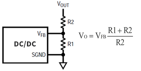
Please tell me how to set the voltage.
In the case of a power supply IC with adjustable output voltage, it can be set by the internal reference voltage (Vref.) and voltage dividing resistors R1 and R2.
Please tell me the pin to control the power on/off.
Depending on the manufacturer and product, the RUN/EN and /SHDN pins are applicable. Please read and confirm the datasheet before use.
How do I calculate the efficiency of a linear regulator?
If the quiescent current is sufficiently small compared to the output current, the efficiency can be obtained by (Equation 1). On the other hand, if the output voltage and the quiescent current of the linear regulator are about the same, it can be calculated using (Equation 2).
output voltage
―――――― … (Formula 1)
input voltage
(output voltage x output current)
―――――――――――――― × (output current + self-consumption current) …(equation 2)
input voltage
What is dropout voltage?
It is the input-output voltage difference of the power supply circuit. If the minimum dropout voltage for proper operation of the power supply is 300mV, it is possible to get an output of less than 1.5V from a 1.8V input. For linear regulators that do not have a specified minimum dropout voltage, the reference voltage is the dropout voltage.
How should the capacitance of the input capacitor be determined?
If the output capacitor has the capacity specified in the datasheet and the output is unstable or the load response is poor, increase the capacity of the input capacitor. After that, check the ESR and if the value is large, consider reducing the ESR.
Since the current capacity of the LDO is insufficient, please tell me how to connect in parallel.
If you simply connect the output of an LDO and use it, the LDO with a small output will act like a load and current will flow into it. The outputs of each LDO must be balanced and equalized, so use ballast resistors at the outputs and connect them in parallel.
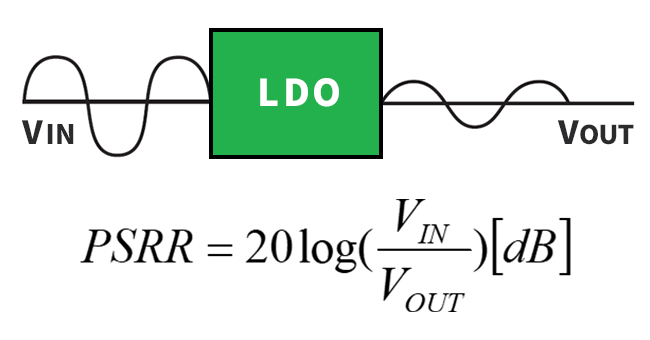
What is PSRR?
PSRR (power supply rejection ratio) is a ratio that indicates how much noise that enters the input is removed without being output to the output. It can be said that the larger the value, the higher the noise reduction ability. When using a linear regulator as a filter, it is recommended to select a product with a large value.
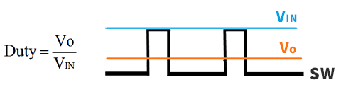
It says to check the duty cycle, what's the problem?
A rough calculation of the duty cycle is output voltage (VOUT) ÷ input voltage (VIN). Since the maximum (MAX.) duty cycle is specified for each product, use it within the specified range of the datasheet. Some products have a minimum (MIN.) value.
For products without duty cycle specifications, please check the switching on-time and off-time specifications. If this value is deviated, the switching cycle becomes unstable and the output voltage becomes unstable. It becomes noticeable when the load current is increased. The Buck Regulator Duty equation is:
How can I make the ripple smaller?
Use ceramic capacitors with small ESR (equivalent series resistance) by increasing the capacity of the output capacitor. In addition, ripple can be reduced by using a power supply IC with a high switching frequency. Note that the higher the switching frequency, the lower the conversion efficiency of the power supply.
What are the advantages and disadvantages of using products with high switching frequencies?
The advantage is that peripheral components such as inductors can be made smaller. Characteristically, the ripple is reduced, the crossover frequency is increased, and the bandwidth is widened, resulting in better load response. The disadvantage is that it becomes difficult to improve efficiency, so attention must be paid to thermal design.
Where are step-up switching regulators used?
It is often used when making analog power supplies from 5V to 12V or 15V. Recently, there are few 5V logic power supplies on the board, so 3.3V is supplied to the board as the main power supply, and the 5V logic power supply is sometimes made with a step-up switching regulator.
What is Ripple?
AC wave-like noise that appears in the input and output of power supplies. In a word, waves. Ripple occurs because switching operation (ON/OFF) is performed in the control of the DC/DC converter. As one of the power supply characteristics, it is desired that the output voltage ripple is small. It can be said that the output voltage is stable when the wave of the output voltage is small.
What is Line Regulation?
This is the amount of change in the output voltage when the input voltage fluctuates. In a system where the input voltage fluctuates, such as a battery, it is necessary to check the power supply used for the core voltage of the FPGA.
What is Load Regulation?
This is the amount of change in the output voltage when the load current fluctuates. When the amount of change in current from a light load to a maximum load, such as an FPGA, is large, the amount of fluctuation in the output voltage will be large. Confirmation is required in such cases.
What is the difference between constant voltage mode and constant current mode?
Constant Voltage Mode (CV) is the operation of buck and boost regulators that power digital and analog circuits. This circuit has the characteristic of outputting a constant voltage even if the load current changes. Constant Current Mode (CC) is the operation of regulators used in LED drivers and battery chargers. This circuit is characterized by a constant current flow to the output even if the load changes.
What is Load Transient Response?
The output voltage overshoots and undershoots when the load current fluctuates abruptly. It is the speed at which the output voltage returns to the set voltage against this sudden load change. Power supplies with fast load response are required for circuits such as FPGAs and CPUs that transition from sleep mode to burst mode.
Regarding the absolute maximum ratings, there are products with a guaranteed junction temperature of 125°C, while the guaranteed case temperature is 150°C. Why is this?
For the guaranteed case temperature of 150°C, the case temperature must not exceed the upper limit of 150°C even when the device is not in operation. For example, if the product is stored in an oven at 175°C for a long period of time, the product cannot be guaranteed. The junction temperature specifies that the junction temperature should not exceed 125°C while the product is in operation. For example, even if the case temperature is 150°C or less, it cannot be used if the calculated junction temperature exceeds 125°C.
I hear that some old power supply ICs cannot support 0.9V output. What determines the minimum output voltage?
It is determined by the reference voltage of the power supply IC. For example, for an IC with a reference voltage of 1.2V, the minimum voltage is set to 1.2V, and 0.9V output cannot be set.
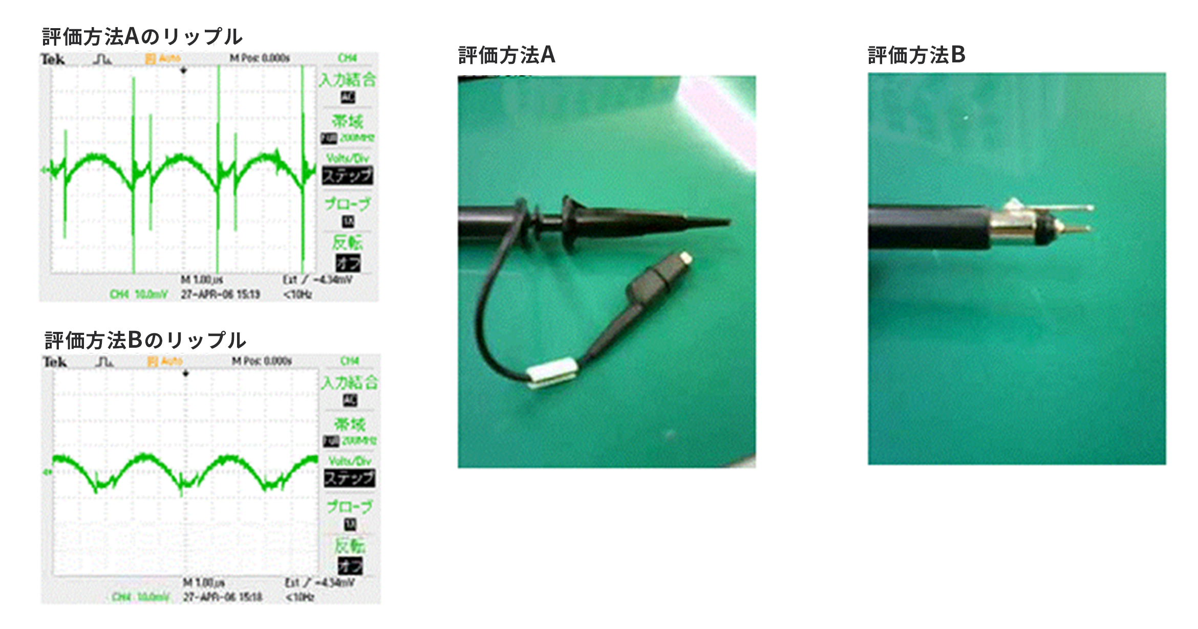
The ripple of the switching regulator is 1V or more. What's causing this?
I'm guessing there is a problem with the measurement method. Measure with the oscilloscope GND wiring as short as possible. Remove the tip of the probe as shown in the picture, and use a socket that shortens the GND to measure. We believe that this measurement method removes the high-frequency noise on the GND line and restores the normal ripple voltage level.
What is the operating temperature range of the power device that has storage temperature (Storage Temperature: -60°C to 150°C) and junction temperature (MAX 150°C) on the date sheet?
The meaning of the temperature range is explained step by step.
◎Storage Temperature
The temperature conditions are the absolute maximum ratings during storage. In terms of practical use, the temperature is the quality-guaranteed temperature of the device when no voltage is applied. For example, it is the temperature range for storing the board after mounting, or the temperature range where quality can be guaranteed when not operating in the usage environment. If you are in a cold area and the voltage is off, there is no problem even if the temperature drops below -40°C. Characteristics can be guaranteed by using a heater to set the temperature within the operation guarantee range when operating.
◎Junction temperature
Power devices must be used so that the junction temperature does not reach the absolute maximum rating. It can be used within the temperature range where the following relationship holds. Operating temperature (ambient temperature) + power device loss × package thermal resistance < junction temperature If the loss x package thermal resistance is within the range of 125°C or less, it can be used.
◎Operating temperature range
Some power devices do not have a specified operating temperature range. The reason is that it can be derived from the junction temperature item formula. The answer to your question is as follows. Operating temperature (ambient temperature) < junction temperature - power device loss x package thermal resistance.
The output voltage is unstable when using a ceramic capacitor for the output capacitor of a linear regulator. Why?
Since ceramic capacitors have a small ESR, it is considered that they oscillate under the condition that phase margin cannot be obtained. Use an aluminum electrolytic capacitor with a large ESR or the like. If the use of ceramic capacitors is essential, select a linear regulator compatible with ceramic capacitors.
Some products have a description to connect the TAB pin of the linear regulator to VOUT. I would like to connect it to the GND of the case, is there any problem?
Please connect the TAB pin linear regulator specified for connection with VOUT to VOUT. Although the TAB pin is not internally connected to VOUT, it is structured so that it cannot be connected to GND. When connecting to a part that is advantageous for heat dissipation, such as the case or GND, it is recommended to electrically insulate the TAB and the board when connecting with an insulating heat dissipation sheet.
Use with the output 3.3V setting for devices that use lithium-ion batteries. Please tell me about a step-down regulator that outputs 3.3V when the input drops to 3.3V, and outputs the same voltage as the input even if it drops below 3.3V.
Select a product with a 100% duty cycle. A slight voltage difference due to loss occurs between input and output, but if the input voltage falls below the output set voltage, a voltage close to the input voltage will continue to be output until the input UVLO (Undervoltage Lockout) voltage. In this figure, the input voltage (red) begins to fall, and after 3.3V, the output voltage (green) also decreases with the same slope as the input. When the input voltage reaches around 2.5V, it exceeds the UVLO threshold and the output turns off.
I tried to get an output of 1A with an input voltage of 5V and an output voltage of 12V using a step-up switching regulator with a built-in 1.2A switch, but the output is only up to about 400mA. Why is it even though it is stated that it is possible up to 1.2A?
The switch current given in the boost switching regulator datasheet is the maximum input current. The formula for calculating the output current of a boost regulator is: output current = input voltage x input current x efficiency ÷ output voltage. In our example, assuming 90% efficiency, 5V x 1.2A x 0.9 ÷ 12V = 450mA.
Even if I try to turn off the power supply with the shutdown pin, the voltage appears on the output pin. Why?
Turning off the shutdown pin (SHDN) stops internal switching action. However, in a boost converter configured as shown below, the output VOUT is connected to the input VIN with an inductor and a diode, so voltage appears at the output pin. To prevent this, select a boost converter with a power FET between the input and output and an input/output disconnect function.
Bug-related Q&A
I hear a noise from the power circuit. What could be the cause?
The configuration of the input filter may have an effect. Please add an electrolytic capacitor with a large ESR as an input capacitor and check if the problem is improved.
When evaluating boards in a constant temperature bath, the power supply circuit burns out frequently. Is the power circuit damaged by the high temperature?
There is a possibility that the wiring that connects the stabilized power supply and the board is long when putting it in the constant temperature chamber. Shorten the wiring of the power supply, or slow down the start-up of the power supplied from the stabilized power supply to check whether the problem can be improved.
When I checked the switching waveform of the power supply circuit, it seems that the switching waveform skips pulses and oscillates intermittently. Please tell me how to deal with it.
Since the load is under light load conditions, there is a possibility that pulse-skipping is operating. Please check the load conditions and then check if the load conditions for pulse skipping apply to the power supply product you are using. If there are no problems, check whether the duty ratio and switching frequency obtained from the input/output voltage are within the Minimum On Time specification of the power supply IC. Pulse skipping may occur even if the Minimum On Time is exceeded.
If you turn on the power immediately after turning off the power, the output of the DC/DC converter on the board will repeatedly turn on and off, and the output will not start up normally. Please tell me how to deal with it.
Immediately after turning off the power, voltage may remain on the output side of the DC/DC converter. In that case, the input will be lower than the output voltage, and the DC/DC converter will be pre-biased and may not start well. As a countermeasure, use a DC/DC converter that can operate even in a pre-bias state, or start after the voltage on the output side is removed.
I got a DC/DC converter evaluation board and am testing the device at low temperatures using cooling spray. It works fine at room temperature, but the output voltage becomes unstable when the temperature is lowered with a cooling spray. Why might the output of a DC/DC converter become unstable at low temperatures?
Low temperatures can change the characteristics of peripheral components (especially capacitors), making the output voltage unstable. The output may become unstable due to leakage current flowing between the pins or to GND. Perform a low-temperature test in a constant temperature bath to see if the same phenomenon occurs.
When I turn on the board, the output of the DC/DC converter does not monotonically increase and the FPGA does not work well. Please tell me about a power supply IC in which the output of a DC/DC converter increases monotonically.
If the output of the DC/DC converter does not monotonically increase, it can be inferred that the rush current is causing the output to become unstable. Select a DC/DC converter that has a soft-start function and can change the start-up time by setting the constants of resistors and capacitors outside the IC.
We received an inquiry from a subcontractor's component mounting line about the frequent occurrence of IC burnout after power-on. I think it's a device problem, so would it be possible for you to analyze it?
If the burnout problem occurs frequently when the power is turned on after mounting, there is a high possibility that the problem is due to board mounting conditions and board design. Check the wettability of the solder with X-rays, etc. After that, it will be the flow to check whether analysis is possible.
The output voltage of the DC/DC converter is unstable. When I checked with another engineer, it seems that the layout of the output capacitor is not correct. I was told. Please let me know the points to be careful about when placing the output capacitor.
Please check the capacity of the output capacitor as it may not be the value recommended by the manufacturer. Also, even if the capacitance of the capacitor matches, please note that the output may become unstable due to differences in the characteristics of the capacitor and placement of the capacitor on the board (mounting on a different surface than the power supply IC).
I hear that the board layout (artwork) is important in the design of DC/DC converters. What kind of problems will occur? Also, what should we refer to when designing?
Various problems can occur. The biggest problem is the possibility of overvoltage breakdown due to layout issues. Also, the output of the power supply may oscillate and produce an unstable output. When designing the layout, refer to the layout of the demo board provided by the manufacturer.
If the board is evaluated with a long power line, the DC/DC converter on the board will be damaged. If the power line is shortened, the problem does not occur at all. What could be the cause?
Damage is thought to be caused by the relationship between the inductance of the power line and the ESR of the input capacitor of the DC/DC converter. If you only use a ceramic capacitor with a low ESR as the input capacitor, if you lengthen the power supply line, voltage overshoot may damage the DC/DC converter, so be careful.
A DC/DC converter generates 0.9V from 12V and supplies it to the IC, but when the 0.9V load current increases, the IC malfunctions.
It turned out that the cause was that 12V switching noise had an effect when the current value increased. I've tried adding an output capacitor to the 0.9V line and putting in a ferrite bead filter, but that doesn't help at all. Please tell me some good countermeasures.
First, if 12V switching noise is the cause, put a ferrite bead on the input side (12V line) of the DC/DC converter instead of the output side. Also, put a GND between the 12V layer and the 0.9V layer to separate them.
In order to evaluate power supply ICs from multiple companies on the same board, I am evaluating them by connecting jumper wires to the legs of the ICs, but the power supply IC is broken. Please let me know if there is a workaround.
If a power supply IC is connected with a jumper, overvoltage will be applied to the IC due to the inductance of the jumper wire. Therefore, the IC is destroyed by overvoltage destruction. Order the evaluation board from the power supply IC manufacturer without connecting with a jumper, and evaluate the IC.
When the board with FPGA came up and turned on the power, it turned out that there was a board that did not work because the power did not start up normally depending on the timing.
The cause is that the overcurrent detection of the power supply module is effective and the power supply does not start up. When I calculated the power consumption of the FPGA, it should be enough for the power supply module installed, but what is the problem?
It is said that the overcurrent detection of the power supply module is effective at startup, so please check once that the power supply sequence of the FPGA is being followed. If the power supply sequence is not followed, a large rush current may flow. If it still does not improve, try using the soft start function of the power supply to reduce the rush current and reduce the output capacitor capacity to see if it improves.
There are boards where PCI-Express Link-Up does not work well. If you increase the power supply voltage, the probability of success will increase. Power supply seems to be the culprit. Please tell me how to deal with it?
Please check the power supply voltage related to PCI-Express near the FPGA. It is highly likely that the required voltage is not being applied due to IR drop on the board. Even if a ferrite bead or 0 (zero) Ω resistor is inserted, an IR drop will occur depending on the resistance value, so please remove it and check if it can be improved by soldering bridges.
I heard that inserting a ferrite bead into the power supply line may deteriorate the signal quality of the digital signal or worsen the wireless characteristics. Is there a possibility that the characteristics will be worsened by inserting a filter?
Anti-resonance frequency points are created on the board by L and C, which may affect the quality of digital and wireless signals, and in the worst case, lead to malfunction of the IC. It is also important to perform PDN (Power Distribution Network) analysis, etc. to check for large anti-resonance points.
The output voltage of the DC/DC converter is unstable. When I checked with another engineer, it seems that the layout of the output capacitor is not correct. I was told. Please let me know the points to be careful about when placing the output capacitor.
Please check the capacity of the output capacitor as it may not be the value recommended by the manufacturer. Also, even if the capacitance of the capacitor matches, please note that the output may become unstable due to differences in the characteristics of the capacitor and placement of the capacitor on the board (mounting on a different surface than the power supply IC).
Macnica power dock service
For more detailed support, we introduce the "power dock service", a technical service related to power supply circuits and board layouts with FPGAs. Please click the banner below.