- Semiconductor BusinessHOME
- Products and Services of Macnica,Inc.
-
technical information

-
Events and Seminars
- Handling Manufacturer
- Support
- Inquiry
- Click here to purchase products
- Semiconductor business e-mail magazine registration
![]()
![]() Narrow down by specifying conditions
Narrow down by specifying conditions
現在2175件がヒットしています。check
This is Sasaki in charge of power supply dock technology.
In this column, I would like to introduce some examples of problems related to power supplies that I encountered multiple times during various customer support sessions.
One day, there was a report that "the power supply of 50% of the boards burnt out during the test process".
There are things you can't understand from a circuit diagram alone...
It is thought that the power supply IC lot is defective, and they are preparing a replacement product and conducting a defect analysis as soon as possible.

(The 50% defect rate is too high for defects caused by ICs...)
Thinking that the problem was something other than the IC, I decided to check the circuit diagram and layout diagram.
When I checked the schematic, there was no particular problem.
It will take time to provide the layout drawing.

Layout drawings are time consuming, so I took pictures instead.
Appearance does not appear to be a problem.
check the photo
surely···.
The IC leads are neatly soldered, and looking at the layout on the board in the photo, there doesn't seem to be any problem. . .
My boss asked me to take an X-ray, so could you take a look at it too?
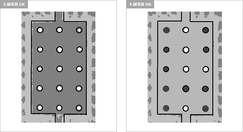
I see, so that's what it was. I know the reason.
really! ?
Looking at the X-ray photograph of the one that is working normally, there is solder on the back of the IC, but the burnt one has no solder from the back of the IC.
Is true. . Did it melt and disappear because it was damaged by fire? ? ?
Cause of power supply burnout
Solder on the back of the power supply IC flows down into the through-hole, resulting in poor solder wettability.
If you look at the X-ray picture of the burnt product, the through holes are black.
This is due to the solder flowing down into the through-holes during reflow.
As a result, the wettability of the solder decreased and the power supply IC burned out.
In such cases, the through-hole design must be optimized for the soldering process.
The point of this time
Pay attention to the through-hole design for heat dissipation on the backside of the IC.
application note
An application note is available for download that introduces three troubleshooting methods for through-hole designs.