- 半導体事業HOME
- マクニカの製品・サービス
-
技術情報

-
イベント・セミナー
- 取扱メーカー
- サポート
- お問い合わせ
- 製品購入はこちら
- 半導体事業のメルマガ登録
![]()
![]() 条件を指定して絞り込む
条件を指定して絞り込む
現在2173件がヒットしています。check
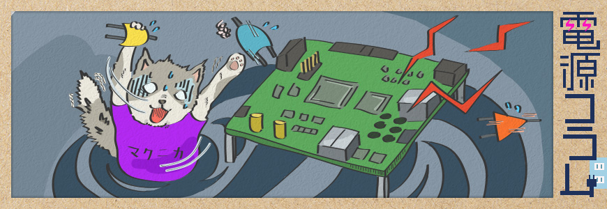
電源ドック技術担当の佐々木です。
このコラムでは、色々なお客様サポートの中で複数回遭遇した、電源に関する不具合事例をご紹介していきたいと思います。
ある日、「DC/DCコンバーターのノイズの影響でボードが動かないので至急サポートして欲しい。」との問い合わせが。
スイッチングノイズの伝達経路は?
詳しい症状はこちら
- 0.9V ラインに高周波のスイッチングノイズがのっている。 ←不具合原因の可能性大
- 同様の組み合わせ(デジタル回路 & 電源)で過去に開発した基板は正常に動作
- デジタル IC の処理速度を上げるとシステムエラーが発生
- デジタル回路の消費電流に対して、DC/DC コンバーターの電力供給能力は十分

IC メーカーが推奨している、『コア電圧 0.9V』の要求仕様は満たしているのに、
デジタル回路の処理速度を上げると、なぜかシステムが止まってしまいます。。。

回路図とレイアウト図も問題ありませんね。
実際に動作異常が発生する瞬間を見せていただけますか?
実機を使って動作異常を確認
0.9V ラインは電圧降下も無く、大きな問題はありませんね。。
やはり、電源のスイッチングノイズが原因でしょうか?
対策としては、ローノイズの DC/DC コンバーターに変更するしかないですかね?
そうなると時間もコストもかかって困っちゃうんだよなぁ。。。
波形を見る限り、この電源が特別大きなノイズを出すとは考えにくいですね。
電源部分だけでなく、基板全体のレイアウトと層構成を見せていただけますか?
基板全体の層構造を確認
なるほど、12V層と 0.9V層が重なっていますね。
これが原因で 12V の入力ラインのスイッチングノイズが 0.9V の層にカップリングしてしまっているようです。
対策として、12V と 0.9Vの層間にGNDを入れるか、DC/DC の入力部分にビーズフィルターを入れてみてください。
はい、やってみます!
上記対策を実施した結果このトラブルは無事収束し、電源 IC の変更もなく、最低限の修正で問題を解決することができました。
デジタル回路が誤動作した原因
DC/DCコンバーターの入力側で発生したスイッチングノイズ
(2つの層が重なっていることで大きな問題に)
今回のポイント
低電圧大電流を必要とするデジタルICを使用する際は、スイッチングノイズの影響を考慮した基板全体の電源設計が必要。