- Semiconductor BusinessHOME
- Products and Services of Macnica,Inc.
-
technical information

-
Events and Seminars
- Handling Manufacturer
- Support
- Inquiry
- Click here to purchase products
- Semiconductor business e-mail magazine registration
![]()
![]() Narrow down by specifying conditions
Narrow down by specifying conditions
現在2189件がヒットしています。check

Recent Altera® FPGAs support PCI Express (PCIe) as standard. When you want to implement PCI Express on an Altera® FPGA, you may wonder where to start. For example,
- Which FPGA Devices Support What?
- How much transfer rate does each FPGA device support?
- How to FPGA design? Do you have a reference design?
I'm sure you have many questions, such as:
The tools used include the Quartus® Prime development software and, in some cases, the Platform Designer system integration tool bundled with Quartus® Prime.
This article introduces the process from selection to an overview of design methods for those who are implementing PCI Express with Altera® FPGAs for the first time.
Step 1: Select the device to use
To get started, visit the PCI-Express IP Support Center page on the Altera® FPGA site. Here you can find an overview of Altera® FPGA's PCI Express solutions, including an overview of the PCI Express protocol, features, device support, getting started guides, and technical support.
By looking at the device support section, you can see which devices support the configuration you want. For example, a PCI Express Gen1 x4 configuration can be achieved with all listed devices. However, if you want to achieve Gen3 x8, only a limited number of devices can achieve it.
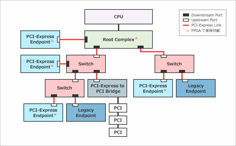
Also, although "Device Configuration and Functional Support" mentions endpoints and root ports, Altera® FPGA PCI Express IP can implement both endpoints and root ports (ports when implementing root complexes). To implement a root complex, you can set the IP core to root port and add control from the host controller.
Step 2: Determine configuration in FPGA by data transfer format
Looking at the list of documents in the Getting Started Guide section, there are documents for Avalon-Streaming (Avalon-ST), Avalon-Memory Mapped (Avalon-MM), and Avalon-MM with DMA. Which one to choose depends on your usage conditions. The differences are as follows:
If you are interested in Avalon-ST or Avalon-MM, please see here.
[FAQ] What is the difference between the Avalon-MM interface and the Avalon-ST interface?
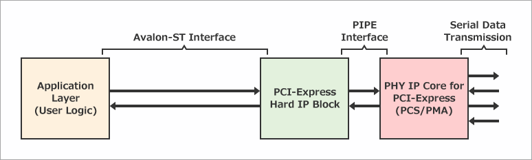
Avalon-ST configuration
The interface on the FPGA fabric side of PCI Express is Avalon-ST. Avalon-ST transfers data in a stream format, with Start-of-Packet (SOP) and End-of-Packet (EOP) indicating the start and end of data. The data is the PCI Express TLP (Transaction Layer Packet) itself, and implementation must be based on a detailed understanding of the TLP as specified by the PCI Express specification. There are no other specification restrictions. Implementation is possible within Platform Designer or without Platform Designer.
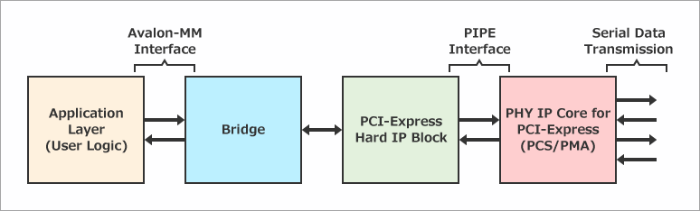
Avalon-MM configuration
The interface on the FPGA fabric side of PCI Express is Avalon-MM. Avalon-MM transfers data in memory-mapped format, and addresses must be specified when sending and receiving data. Implementation requires the use of Platform Designer, which requires address conversion between Platform Designer's internal address space and the host PC's address space. However, it is relatively easy to implement without the need to understand the details of TLP. Specification limitations include fewer tag support than the Avalon-ST configuration, single-function support, no ECRC forwarding support, and no support for Expansion ROM.
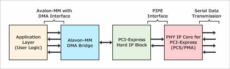
Avalon-MM with DMA configuration
The basic configuration is the same as the Avalon-MM configuration, but for more efficient transfers, a DMA engine is implemented in the core. The limitations of the specification, combined with the limitations of the Avalon-MM configuration, result in a configuration that cannot achieve a root port and has limitations on TLP support. For details, please refer to the comparison table in each document.
Based on the above, decide which configuration to choose depending on the case you want to realize.
case 1
When implementing a root port/endpoint with a single function, an Avalon-MM configuration is typically used. If you want to use DMA, you can achieve high-speed DMA transfers by using modular Scatter-Gather Direct Memory Access (mSGDMA), which is included as standard with Platform Designer. Although there are limitations, such as limited tag support, only single-function support, no support for ECRC forwarding, and no support for Expansion ROM, we recommend using this configuration unless these limitations are met.
case 2
In cases where a root port/endpoint is implemented as a multi-function device, or when Platform Designer is not desired, implementation using the Avalon-ST configuration is required. You must understand the details of the TLP and implement the Avalon-ST packet in your own logic.
case 3
For example, if you want the most efficient transfer possible with a Gen3 x8 configuration, choose the Avalon-MM with DMA configuration. Because the DMA engine is inside the Avalon-MM bridge, more efficient transfers are possible.
Step 3: Experiment with the Reference Design
Below is a list of reference designs for Avalon-MM configurations.
Altera FPGA Developer Site
PCI Express* IP Support Center - 2. User Guides and Reference Designs
Below is the design for Avalon-MM with DMA.
Cyclone® V FPGA – PCIe* 2.0 x4 Avalon® Memory-Mapped DMA Design Example
Cyclone® V FPGA – PCIe* 2.0 x4 Avalon® Memory-Mapped DMA On-Chip and External Memory Design Example
Arria® V GX FPGA – PCIe* 2.0 x4 Avalon® Memory-Mapped Interface DMA Design Example
Gen3x8 Avalon-MM DMA Reference Design with Internal Memory (AN 690)
Gen3x8 Avalon-MM DMA with External DDR3 Memory (AN 708)
Gen3x8 Avalon -MM DMA with External DDR3/DDR4 Memory (AN 829)
Each reference design is designed to run on the evaluation board for each Altera® FPGA device series. Designs are available for the following development kits. Software samples are also available, so if you have an evaluation board, you can immediately check operation on the actual device.
Reference information
Avalon-ST configuration implementation documentation
You can use the reference designs that can be generated in Quartus® Prime. For the Arria® 10 FPGA, select the Arria 10 Hard IP for PCI Express from the IP Catalog and launch it. Click the Example Designs tab to generate a Quartus® Prime project. This design uses an Avalon-ST configuration.
PCI Express with Altera® FPGA (Avalon-ST Edition)
Avalon-MM configuration implementation documentation
PCI Express with Altera® FPGA (Avalon-MM Edition)
DMA Transfer Using PCI Express Hard IP
Click here for recommended articles/materials
PCI Express with Altera® FPGA (Avalon-ST Edition)
PCI Express with Altera® FPGA (Avalon-MM Edition)
FPGA PCI Express Design & Debug Guidelines
Altera® FPGA Development Flow