- Semiconductor BusinessHOME
- Products and Services of Macnica,Inc.
-
technical information

-
Events and Seminars
- Handling Manufacturer
- Support
- Inquiry
- Click here to purchase products
- Semiconductor business e-mail magazine registration
![]()
![]() Narrow down by specifying conditions
Narrow down by specifying conditions
現在2183件がヒットしています。check

Hello. I'm Hanako Altera, who provides technical support for Altera® FPGA products at Macnica.
The user designs the logic circuit inside the FPGA from scratch. Therefore, it is impossible to design without knowing anything at all.
So what exactly should we learn?
Note: Intel's Programmable Solutions Group became Altera®, an Intel company, in January 2024.

For now, let's start by learning about this.
- デジタル論理回路についての知識
- ハードウェア記述言語とのコーディング能力
- I/O規格についての知識
- Knowledge of static timing analysis (STA: Static Timing Analyzer)
If you know more, it will be more convenient, but you can start designing if you know this area first.
Let's talk a little bit more about each.
デジタル回路についての知識
FPGA ではデジタル回路を設計します。ちなみに、FPGA の業界ではデジタル回路を 論理回路 と言うのが一般的です。
論理回路を構成するには、
- AND、OR、NOT、フリップフロップなどの基本論理回路
- 2進数、2進数演算
- 組み合わせ回路、順序(フリップフロップ)回路
- 同期式順序回路、非同期式順序回路
このあたりのことを勉強しておけば、基本的な回路は設計できます。(みなさんからリクエストがあれば、この辺の技術記事も書きますよ。)
ハードウェア記述言語のコーディング能力
論理回路を設計するためには、ハードウェア記述言語のコーディング能力が必要です。ハードウェア記述言語は通称 HDL (Hardware Description Language) と言われ、現在では主に以下の3種類が使用されています。
- VHDL(ブイエイチディーエル)
- Verilog-HDL(ベリログ・エイチディーエル)
- SystemVerilog(システム・ベリログ)
通常 ユーザーはどれか1種類を使用して設計します。(それぞれの特徴については、また別の機会に紹介します。)どのタイプの言語を選択するかは個人の自由です。会社で決められている人もいれば、設計依頼元の注文によって使い分けるために両言語をマスターする人もいます。それらの言語で、実現したい論理回路を記述します。
Learn basic grammar first. After that, please get used to “expressing logic circuits in language” by imitating sample circuits. Learning the grammar of a language is not that difficult. Rather than that, you may be more worried about how to express the logic circuit you want to realize in a language.
Language design does not describe the smallest unit of gate logic such as AND, OR, and flip-flops as in schematic (circuit diagram) design, but describes “circuit behavior” on a slightly larger scale.
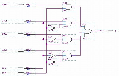
For example, Figure 1 shows a 4-input 1-output multiplexer (selector) configured with gates.
一方、同じ回路を VHDL で記述するとこのようになります。
Library ieee;
use ieee. std_logic_1164.all;
entity mux4to1 is
port (
     data :in std_logic_vector (3 downto 0);
     sel :in std_logic_vector (1 downto 0);
     q:out std_logic
     );
end mux4to1;
architecture logic of mux4to1 is
begin
  process (data,sel)
  begin
   case sel is
     when "00" => q <= data(3);
     when "01" => q <= data(2);
     when "10" => q <= data(1);
     when others => q <= data(0);
   end case;
  end process;
end logic;
There are no AND or NOT gates like in Figure 1, right?
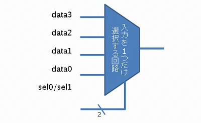
When you hear the word “4-input, 1-output multiplexer,” the image below probably comes to your mind first. The user describes what kind of input they want to operate (output) and let Quartus® Prime think about the gate configuration inside the box. This is language design!
論理回路設計を学ぶ本やサイトを参考にする場合には、言語で設計することを前提としたものを見てください。そうでないと、せっかく効率的に論理回路を書ける言語を使っているのに、論理を式で表して回路記号(AND や OR)を並べて設計するような効率の悪い設計になってしまいます。基礎の勉強は大切なことですが、実務で求められているところはそこではありません。“動くもの(論理回路)を作る” と言うことが重要なんです。
とは言え、まずは言語に慣れましょう。その手始めに、“無料で受講できるトレーニング・コンテンツ” をご紹介します。
| トレーニング・コース名 | Overview |
| VHDL Basics (68 minutes) (From the Altera® website) [Japanese/Free] |
Official online training from the manufacturer. Learn about the VHDL language and examples of its use in logic design. ★Related information★ Get free Altera® FPGA technical training |
| Verilog HDL Basics (49 minutes) (From the Altera® website) [Japanese/Free] |
Official online training from the manufacturer. Learn about the Verilog HDL language and its use in logic design. ★Related information★ Get free Altera® FPGA technical training |
| はじめてみよう!VHDL はじめてみよう!Verilog-HDL [日本語/無料/演習問題つき] |
はじめて VHDL、Verilog-HDL でハードウェア論理回路の設計を行う方向けのページです。基礎の基礎から学習でき、演習を実施して理解を深めることができます。 |
ハードウェア記述言語の使い道は、論理回路を記述する以外にもう一つあります。”記述した論理回路のシミュレーション(動作検証)を実施するための言語”、いわゆる “テストベンチ” を記述するために使用します。
シミュレーションについては、下記ページをご覧ください。
テストベンチの記述については、下記ページをご覧ください。
I/O 規格についての知識
FPGA はデジタル IC です。I/O ピンに入力してきた信号(受信)に対して、それが「High(1)」なのか「Low(0)」なのかを判断し、接続先の IC に信号を出力(送信)することで、「High(1)」か「Low(0)」かを判断させ、周辺デバイスと通信します。High、Low とひとことで言っても、実際基板上では電圧値が関係します。“何V(ボルト)以上が High、何V以下が Low” と言うような電圧値の範囲に規定を設け、それぞれに名称を付けたもの、それが I/O 規格 です。
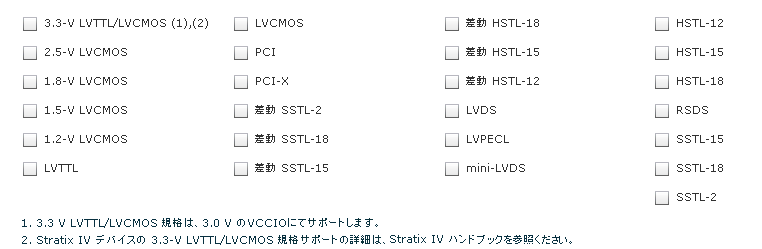
There are various types of I/O standards, and currently Altera® devices support a variety of I/O standards, including single-ended and differential standards (see the figure below for some examples). However, not all families support all of the following, so please check the handbook for each family.
先程お話しした “何V(ボルト)以上が High、何V以下が Low” と言うのはシングルエンド規格の考え方で、1つの信号がその規格で定められた電圧値よりも高いか低いかで High か Low かを判断させます。シングルエンド規格には LVTTL、LVCMOS などがあります。また、シングルエンド規格の中には、外部からリファレンス電圧を供給し その基準値との差で High か Low かを確定する規格もあります。
LVDS, LVPECL, etc. are differential standards. The voltage difference between the two signals determines whether it is high or low depending on whether it is above or below a specified value.
When developing an FPGA with Quartus® Prime, you assign the input, output, and bidirectional pins of the created logic circuit to each pin of the target device. At that time, you can optionally set not only the pin number but also which I/O standard you want each pin to comply with. Therefore, users should be aware of the characteristics of the required I/O standard.
FPGAs can support multiple I/O standards on a single chip. This is because FPGAs have separate power supplies for internal operation (commonly known as core power supplies) and power supplies for I/O terminals to communicate with external devices (commonly known as I/O power supplies). The area (group) of I/O pins that can be driven by each I/O power supply is called an “I/O bank”, and Altera® FPGAs have multiple I/O banks on a single chip. Because different power supply voltages can be supplied to each I/O bank, FPGAs can connect to various peripheral devices with different I/O standards on a single chip.
Users must determine the I/O standard of the peripheral device to be connected to the FPGA, check the electrical characteristics of the I/O standard, and select an FPGA family that can support the I/O standard. Users must also download the data sheet of the FPGA they have selected (or will select) from the Altera® website and check the DC characteristics of the inputs and outputs.
Knowledge of static timing analysis (STA: Static Timing Analyzer) and timing constraints
Timing analysis is to check whether the logic circuit you created operates "correctly" at the required clock frequency, and other timing specifications are satisfied. In contrast to simulation, which uses a simulator such as QuestaSim to simulate the operation of a circuit using input signal data (also called test patterns or test benches), a method that does not use test patterns but analyzes (compares and verifies) against timing requirements (constraints) set by the user is called "static timing analysis."
FPGA circuit elements have inherent delays, so if the required clock frequency is high or the scale of the logic circuit is large, part of the logic circuit may not work. Therefore, we have to perform timing analysis and confirm that it works correctly according to the specifications. It is no exaggeration to say that if timing analysis is neglected, it is not an exaggeration to say that FPGA will not work on the actual device. STA is one of the important tasks in current FPGA development.
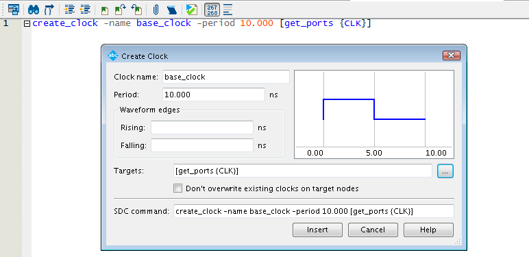
スタティック・タイミング解析をするには、ユーザーの回路に対するタイミング要求情報(タイミング制約)が必須です。そのタイミング制約を FPGA 開発ツールである Quartus® Prime に対して指示することで、ツールはそれを目標値として論理合成や配置配線(いわゆる “コンパイル”)を実行します。Quartus® Primeはタイミング制約に、ASIC 開発で標準的に使用されている “SDC(Synopsys Design Constraints)” ファイル・フォーマットを採用しています。
最も基本的なタイミング制約の例は、クロック周波数の指定です。これ以外にも、設計要求に応じてさまざまな制約が必要です。例えば、FPGA (ユーザー回路)の入出力ピンには入出力データの遅延制約が必要ですし、論理回路に複数のクロックがあれば、そのクロック同士の相関関係を制約として定義することが必要です。その内容を SDC ファイルに記述します。
You don't have to worry about "Do I have to learn SDC in addition to writing logic circuits in HDL?" SDC doesn't have to be learned from scratch like an HDL language. The development software Quartus® Prime has a dedicated editor for writing timing constraints (SDC), and you can easily write commands by entering the necessary information in the prepared dialog Box.
However, before writing SDC, you need to understand the basic concepts of timing (such as setup time and hold time). If you don't know this, you won't know what kind of constraints to write, and you won't get correct analysis results unless you provide appropriate timing constraints according to the circuit structure.
Timing analysis is an essential step in FPGA design. Learn about timing constraints and analysis to ensure a properly functioning product.
Hanako's recommendation♪
An online seminar for beginners on timing constraints and analysis is currently being held.
For more information, please check the page below.
[Online Seminar] Altera® FPGA Timing Analysis - Introduction
今回は、どんなことを勉強しておいた方が良いのか ザックリとご紹介しました。これをきっかけに、知識を徐々に深めて行ってください。
次回は、FPGA 開発の流れ(手順)をご紹介します。
Note:
本記事では 読者に親しんでいただくためメーカーサイトは日本語ページをご案内していますが、併せて英語ページも必ずご確認ください。日本語ページは情報の更新が遅れる場合がありますので注意してください。サイト内の言語切り替えは、ページ下の REGION(地域)により行えます。なお、言語を切り替えてもすべてのページが日本語になるわけではありませんのでご了承ください。
Click here for recommended articles
ほんとのほんとの導入編 その1.FPGA 開発をはじめるための環境づくり
ほんとのほんとの導入編 その2. FPGA 開発をはじめるために準備するもの
ほんとのほんとの導入編 その3. FPGA 開発をはじめるために必要な知識
ほんとのほんとの導入編 その4. FPGA 開発の流れ
ほんとのほんとの導入編 その5. 役立つコンテンツの紹介