
![]()
![]() Narrow down by specifying conditions
Narrow down by specifying conditions
現在1889件がヒットしています。check


This "Let's start! VHDL <with exercises>” is for users who are designing hardware logic circuits in VHDL for the first time. You can learn from the basics of the basics, and you can practice and deepen your understanding.
Overview
"VHDL Introductory Trial Course Workshop" is a workshop held by Macnica group 's Altima Corporation Corporation (currently Macnica Ultima Company) and Elsena Inc. until March 2016.
Due to the end of the regular event, we have decided to renew it and post the same content on the web page.
The target audience, concept, and agenda of this workshop are as follows.
| Target audience | People who are new to digital logic circuit design with VHDL |
| concept | Get an overview of VHDL and learn basic writing techniques |
| agenda |
Language design overview ・ Simple combinational circuit ・ Complex combinatorial circuits ・ Sequential circuit - Calling sub-blocks |
マテリアル
We offer a wide variety of materials here.
Download textbooks, practice manuals, and practice data to learn at your own pace.
| text |
Click to browse or download
|
説明が簡潔にまとめられたテキストです。 The supplementary explanation is also written in spoken language, so it is very easy to understand. |
| exercise manual |
Click to browse or download |
By doing exercises based on the contents of the text, the degree of understanding increases. Please use it together with the following exercise data. Questa or ModelSim (both with Intel FPGA Edition) are required for this exercise. This manual is based on the ModelSim-Altera Edition, but the GUI menus are the same as those of Questa, so you can use them interchangeably. Intel FPGA Starter Edition is free to use. (Questa-Intel FPGA Starter Edition must be licensed and configured for free: see here) |
| exercise data |
Click to download |
Extracting the zip file will generate an exe file. Run the exe file and extract it to any folder. The default is a specification that expands to C:\lab\verilog_lab. |
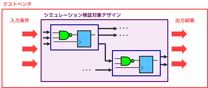
テストベンチ(シミュレーションするならテストベンチが必要!)
<Importance of design logic verification and testbench>
As you all know, hardware description languages (HDL) such as Verilog-HDL and VHDL are the mainstream for FPGA development (logic circuit) design.
Before compiling and debugging on the actual machine, verification work is required to confirm that the design designed in HDL operates correctly. A logical verification of a design involves performing a simulation, but in order to perform a simulation, a "test bench" that describes the input conditions (test conditions) to the design is required separately from the design. And the testbench will be described mainly in HDL by the designer as well as the design.
Before you create a testbench, you need to think about what you are verifying, and you must know how the design under test should behave. Please understand them properly before creating a testbench.
<Relationship between testbench and design (circuit)>
Hierarchical design techniques are mainly used to create designs (logic circuits) in FPGAs. Hierarchically speaking, the testbench resides at a higher level of hierarchy than the design under test (typically at the top level) of the FPGA design. Within the testbench, the input conditions (such as clock inputs, reset inputs, and other inputs) to the design under test are described in HDL and input to the design under test in the FPGA design located in the lower hierarchy. The input signal passes through the created design, the result is output, and by checking the result with the simulator, it is possible to judge whether the created design operates correctly.
The following page explains how to write a basic VHDL testbench.
Coffee break: simulator

To simulate your design, you need a simulator.
Questa - Intel® FPGA Edition is recommended for Intel FPGA users.
The following document consists of ModelSim-Altera, the predecessor tool of Questa - Intel® FPGA Edition, but the operation of the tool is the same, so you can refer to it as it is.
ModelSim-Altera Edition - RTL simulation (VHDL)
Note that Quartus® Prime Standard Edition has a simulation method called "NativeLink Simulation".
Please see the following content for details.
Solve Your Intel® FPGA Functional Simulation with NativeLink