- Semiconductor BusinessHOME
- Products and Services of Macnica,Inc.
-
technical information

-
Events and Seminars
- Handling Manufacturer
- Support
- Inquiry
- Click here to purchase products
- Semiconductor business e-mail magazine registration
![]()
![]() Narrow down by specifying conditions
Narrow down by specifying conditions
現在2149件がヒットしています。check


hello.
My name is Hanako Altera and I provide technical support for Altera® FPGAs at Macnica.

This page explains how to insert Nios® V into an Altera® FPGA and make it blink.
So far, we have performed steps 1 to 6 of the following steps. (For details, see Part 1: Hardware Development.)
In this Part 2: Software Development, we will introduce operations7 to 11.
Nios® V Development Flow (Reprint)
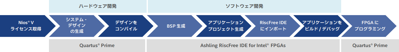
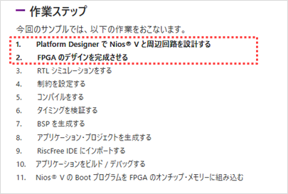
Work steps (reposted)
1. Designing Nios® V and peripherals with Platform Designer
2. Complete the FPGA design
3. RTL Simulation
4. Set constraints
5. Compile
6. Verify timing
<※ Please see the following steps this time.>
8. Generate the application project
10. Build and debug your application
11.Install the Nios® V Boot program in the FPGA on-chip memory
<Notes> For detailed operations of Quartus® Prime, please refer to Altera® FPGA development flow.
Note that steps 7, 8 and 10 (build only) have already been partially performed in "3. RTL Simulation" in Part 1: Hardware Development.
Here, we will introduce the operation flow, taking into account the possibility that hardware development and software development may be done by different designers.
If you have already followed the flow in Part 1, please check each task in Part 2 and decide for yourself whether to "skip" or perform it.
![]() Also, in the latter half of the page, ® This is useful if you have changed the V Boot program. "Time-saving update method" We also introduce the following. It's a must-see!
Also, in the latter half of the page, ® This is useful if you have changed the V Boot program. "Time-saving update method" We also introduce the following. It's a must-see!
7. Generate the BSP
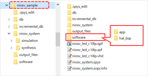
Quartus® Manually create a workspace (folder) for software development within the Prime project folder.
For this example, create a software folder.
Additionally, create a folder for your application project (app) and a folder for your BSP (hal_bsp) in the software folder.
To generate a BSP (Board Support Package), click Start ➤ Open the Altera <version.build_number> <Standard or Lite> Edition folder and click Nios V Command Shell (Quartus Prime <version>) to open the Nios V command shell Start the program.
Enter the following command in the Nios V command shell and specify the Quartus® Prime project folder as the current directory.
cd C:\AlteraFPGA_prj\niosv_sample
Enter the following command in the Nios V command shell to launch the BSP Editor.
niosv-bsp-editor
BSP Editor File menu ➤ New BSP… After selecting, click the button next to the SOPC Information File Name field to specify the hardware information (.sopcinfo file) to be used in the BSP Editor, then click the [OK] button in the New BSP window.
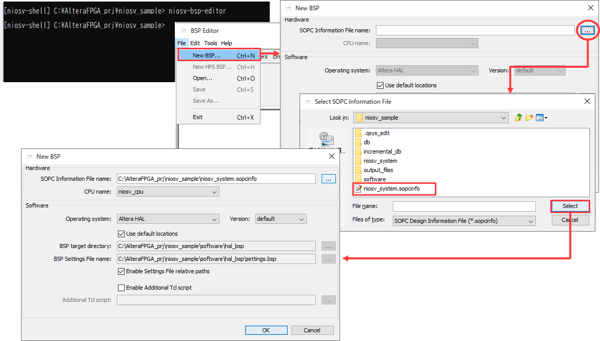
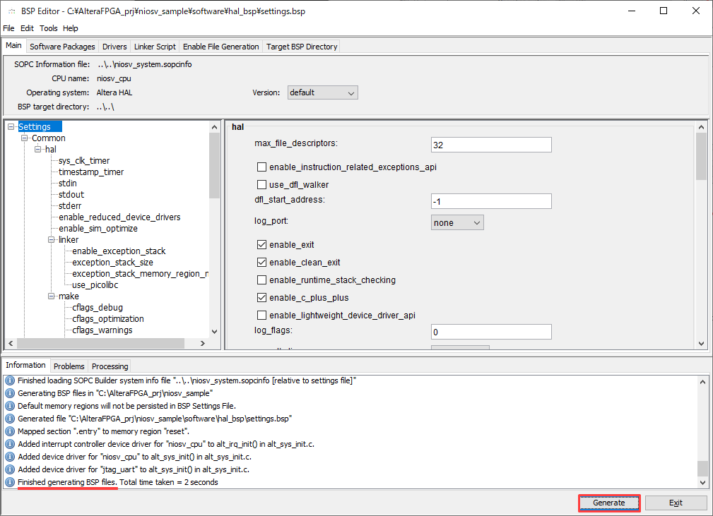
The BSP Editor GUI will be displayed. In this example, no editing will be performed, so click [Generate] in the bottom right of the GUI.
In the Information tab Finished generating BSP files. After confirming that is displayed, click [Exit].
8. Generate the application project
Nios ® created in advance Move the V Boot program (C source file) to the software/app folder you just created.
For this example, save the file as presspb_led_niosv.c.
Next, enter the following command into the Nios V Command Shell:
# Generate the application project files
niosv-app --bsp-dir=software/hal_bsp --app-dir=software/app --srcs=software/app/presspb_led_niosv.c --elf-name=presspb_led_niosv.elf
# Building the application project
cmake -G "Unix Makefiles" -DCMAKE_BUILD_TYPE=Debug -B software/app/build/Debug -S software/app
Enter the following command into the Nios V command shell, then close the shell window.
exit
9. Import into RiscFree IDE
Windows Start ➤ Open the Altera <version.build_number> <Standard or Lite> Edition folder and click Ashling RiscFree IDE for Altera (Quartus Prime <version>) to launch the RiscFree IDE.
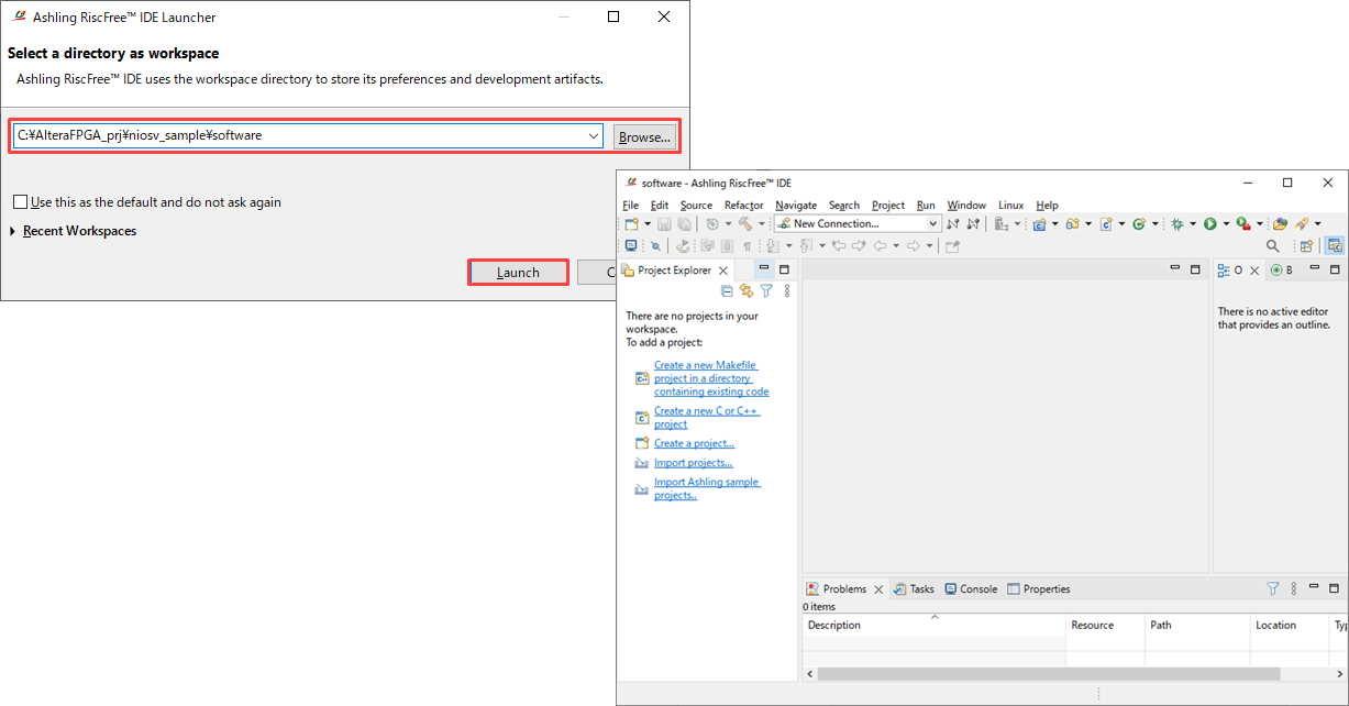
Use the [Browse] button to specify the workspace (software folder) for software development, and click the [Launch] button.
The RiscFree IDE GUI will start.
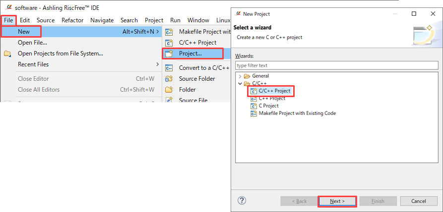
RiscFree IDE File menu ➤ New ➤ Project Select and from the window that appears C/C++ Project After selecting (in the C/C++ folder), click the Next button.
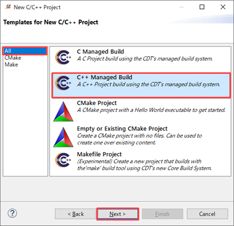
In the New C/C++ Project window that appears, select All from the left frame, select C++ Managed Build from the right frame, and then click the [Next] button.
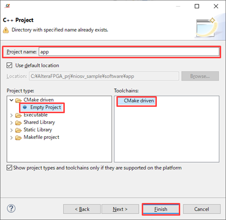
In the C++ Project window that appears, set the following items:
Project name: app
Project type: CMake driven > Empty Project
Toolchains: CMake driven
10. Building and debugging your application
10-1. Build the application
After importing the application project, right-click the app project and select Build Project.
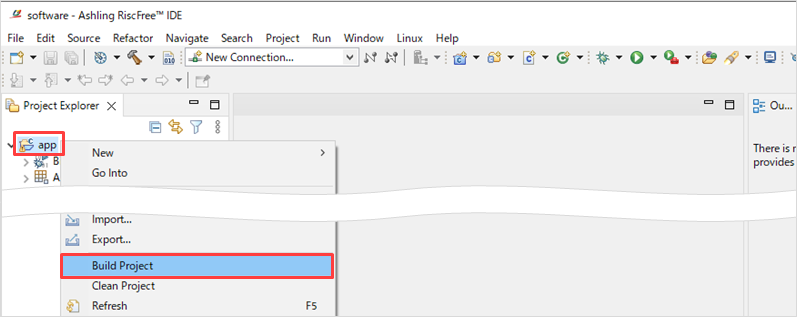
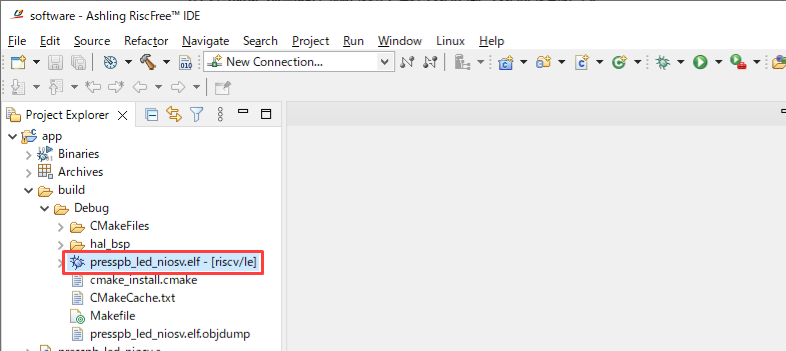
The C source code is built and an executable file .elf is generated.
10-2. Debugging your application
Run the elf file generated by Build Project on the FPGA on the evaluation board to check its operation.
10-2-1. FPGA configuration
Download the hardware program sof file to the FPGA.
<Notes>
Cyclone® 10 LP Evaluation Kit users should set DIP switch SW1.4 to On in advance.
In addition, please install the device driver for USB-Blaster II before using this board.
[Reference information] Installing the USB-Blaster II driver
Connect the mini USB (Type-B) of the cable included with the Cyclone® 10 LP Evaluation Kit to the evaluation board, and then connect the black connector of the USB cable to the PC. This will supply power to the board.
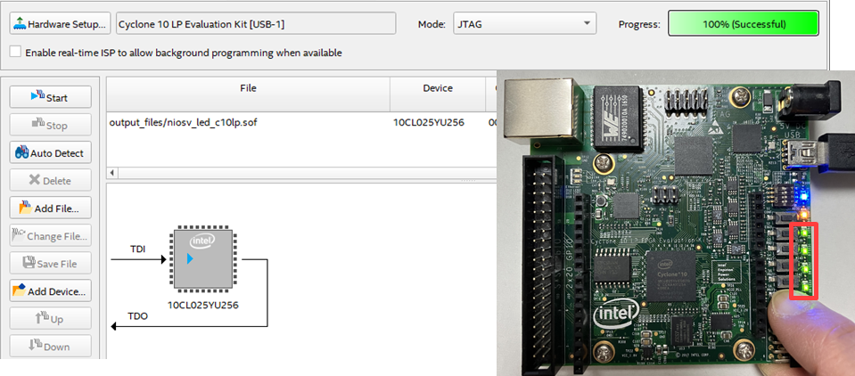
Quartus® From the Prime menu: Programmer Start the program.
Tools menu➤ Programmer
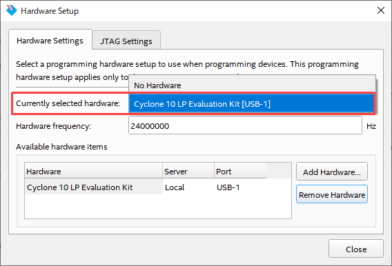
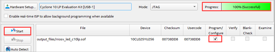
Click the Hardware Setup button in the Programmer window and select Cyclone 10 LP Evaluation Kit.
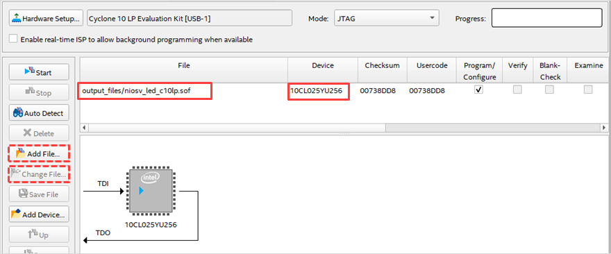
In the Programmer window, select JTAG from the Mode pull-down list.
The niosv_led_c10lp.sof file generated by compiling with Quartus Prime is already registered in the File column, and the FPGA model number specified in the project (10CL025YU256 in this example) is displayed in the Device column.
<Notes>
If the sof file is not registered, click the Add File button, select // Quartus® Prime project folder/output_files/niosv_led_c10lp.sof, and click the Open button to register it in the File field. Alternatively, if another sof file is registered, select that file, click the Change File button, and specify // Quartus® Prime project folder/output_files/niosv_led_c10lp.sof instead.
Check the Program/Configure option on the right side of the niosv_led_c10lp.sof line in the Programmer window and click the [Start] button.
Download the hardware program.
The Progress bar will reach 100% and the Messages window (System tab) in Quartus® Prime will display the message Info: Successfully performed operation(s).
Once confirmed, the download is complete.
10-2-2. Juart-terminal registration
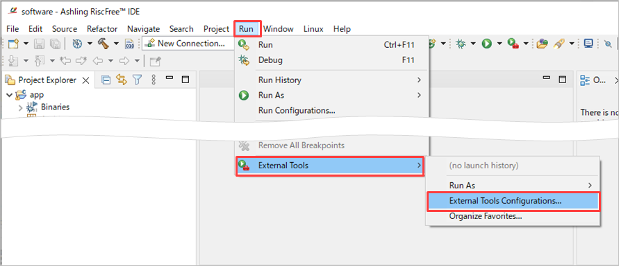
RiscFree IDE does not have a JTAG console, which is a UART terminal, so you need to register an external tool to use the JTAG console.
Launch External Tools Configurations from the following menu.
Run Menu➤ External Tools Configurations...
Highlight Program on the left side of the External Tools Configurations screen and click the New launch configurations icon in the top left.
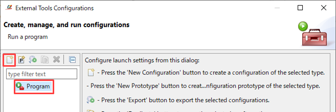
In the GUI that appears, register juart-terminal.
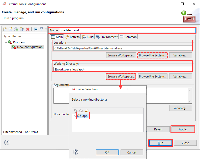
Name: juart-terminal
Location: Absolute path of juart-terminal.exe (use the [Browse File System...] button)
Example) C:\altera\24.1std\quartus\bin64\juart-terminal.exe
Working Directory: Click the [Browse Workspace...] button and select app in the Folder Selection window.
Click the [Apply] button at the bottom right of External Tools Configurations to register the information, then click the [Run] button to execute the configuration.
10-2-3. Start Run Configuration
To download the software program elf file to the FPGA on the Cyclone® 10 LP Evaluation Kit, right-click the app project and select the following menu.
Run As ➤ Run configurations...
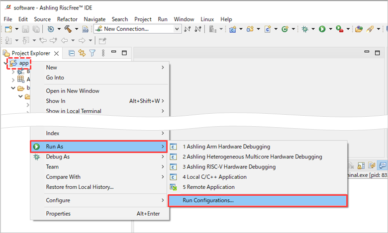
In the Run configurations window, double-click Ashling RISC-V Hardware Debugging.
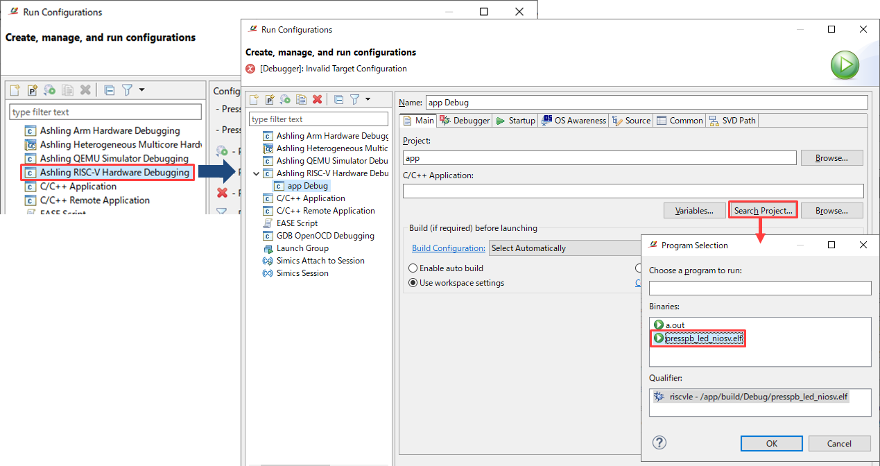
Click the [Search Project...] button in the Main tab, select presspb_led_niosv.elf from the Program Selection window, and click the [OK] button.
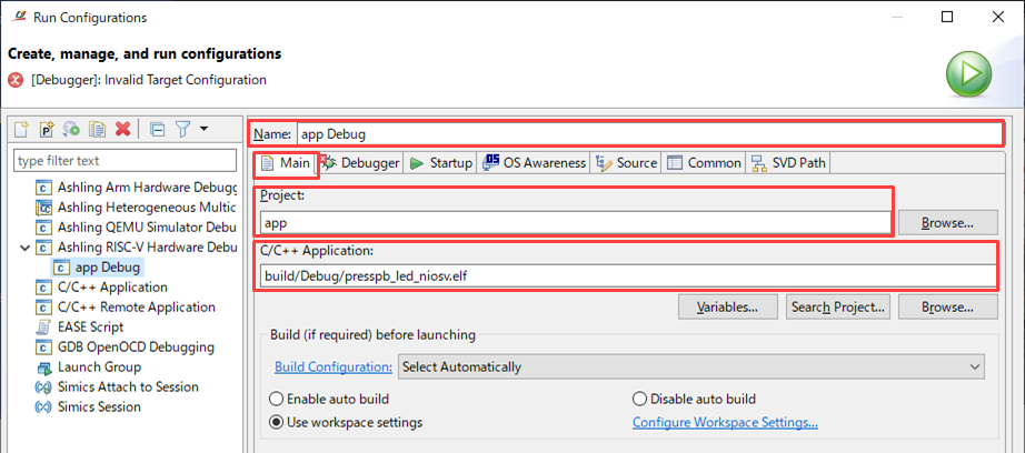
On the Main tab, verify that the following is reflected:
Name: Enter any name (in this example, app Debug)
Project: app
C/C++ Application: build/Debug/presspb_led_niosv.elf
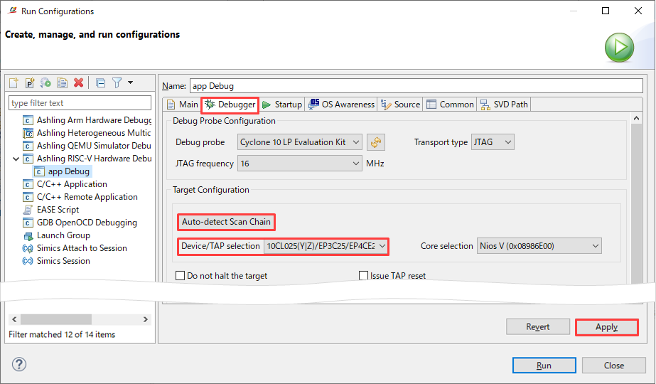
Switch to the Debugger tab, click the [Auto-detect Scan Chain] button, and once you have confirmed that 10CL025(Y|Z) is detected in the Device/Tap selection field, click the [Apply] button at the bottom right.
10-2-4. Run As
Click the Run button in the bottom right of the Run Configuration window.
When the program is executed, the message "Hello from Nios V!!" specified by the alt_printf function will be displayed in the RiscFree IDE Console.
You can also confirm that when you press the push button [PB3] on the evaluation board, the four LEDs light up, and when you release [PB3], all the LEDs turn off.
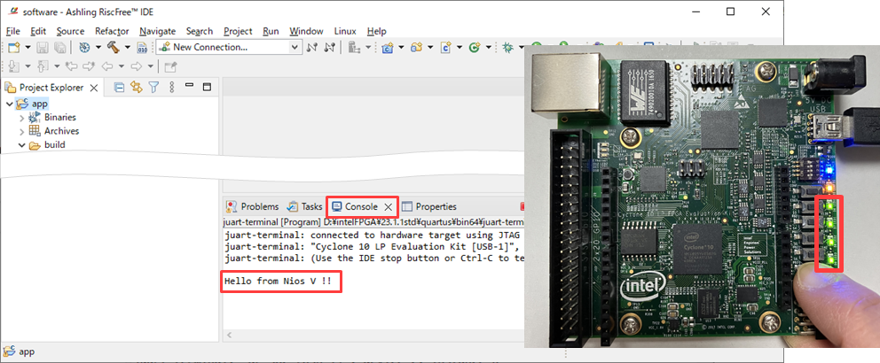
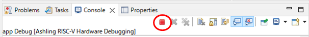
Once you have finished checking the operation, click the ■ button in the Console of the RiscFree IDE to terminate the program.
Select RiscFreeIDE File menu➤ Exit to end RiscFree IDE operation.
11. Install the Nios® V Boot program in the FPGA on-chip memory
Now that the software program works as expected, let's embed this Boot program into the FPGA's on-chip memory.
11-1. Converting the Nios® V Boot program to a hex file
Open the Windows Start ➤ Altera <version.build_number> <Standard or Lite> Edition folder and click Nios V Command Shell (Quartus Prime <version>) to launch the Nios V command shell again.
Enter the following command in the Nios V command shell and specify the Quartus® Prime project folder as the current directory.
cd C:\AlteraFPGA_prj\niosv_sample
Next, enter the following command to convert the elf file to a hex file.
elf2hex app/build/<user_applicatio>.elf -o <hex_output_file>.hex -w <On-Chip RAM data width> -b <On-Chip RAM base address> -e <On-Chip RAM end address>
example)
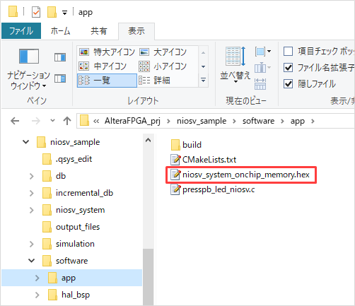
elf2hex software/app/build/Debug/presspb_led_niosv.elf -o software/app/niosv_system_onchip_memory.hex -w 32 -b 0x00010000 -e 0x00019FFF
<Notes>
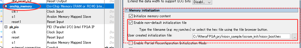
The initial value settings of the on-chip memory created by Platform Designer are the defaults.
memory content = On), the hex file name should be niosv_system_onchip_memory.hex.
If you have specified a file other than the default by setting Enable non-default initialization file = On,
Specify the elf2hex command with -o, followed by the desired filename and path.
Example) elf2hex software/app/build/Debug/presspb_led_niosv.elf -o ocram_init/niosv_boot.hex -w 32 -b 0x00010000 -e 0x00019FFF
11-2. Create meminit.qip, register it in the Quartus® Prime project, and compile it.
<Notes>
If the initial value setting of the On-chip Memory created in Platform Designer specifies a file other than the default (i.e. Enable non-default initialization file = On), it is not necessary to creatememinit.qip. Therefore, skip steps ① to ③.
① In order to reflect the hex file of the Nios® V Boot program that we created earlier as the initial value of the FPGA internal memory (the On-Chip Memory of the Nios® V system),
Enter the following constraints into a text file:
set_global_assignment -name SEARCH_PATH $::quartus(qip_path)
(![]() meminit.qip (sample description)
meminit.qip (sample description)
② Name the filememinit.qip and save it in the same folder as the Nios® V Boot program hex file.
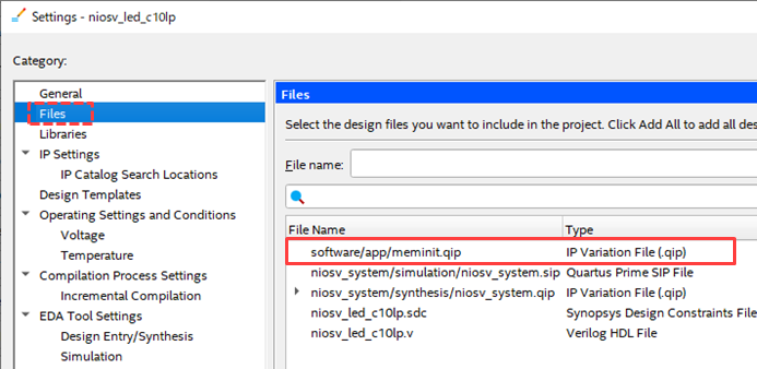
③ Add meminit.qip to the project from the following menu in Quartus® Prime.
I will register additionally.
Projectmenu➤ Add/Remove Files in Project
④ Run compilation in Quartus® Prime.
Processingmenu➤ Start Compilation
Once compilation is complete, a .sof containing the Nios® V Boot program will be generated.
11-3. Write to FPGA and verify on actual device
Launch the Quartus® Prime Programmer to write the .sof.
You can confirm that when you press the push button [PB3] on the evaluation board, the four LEDs light up, and when you release [PB3], all the LEDs turn off.
Now, the Nios® V Boot program is included in the sof file!
If you need a programming file for the FPGA configuration ROM, please use the Quartus® Prime Convert Programming Files function to generate a file based on this sof file.
This completes the Nios® V LED blinking process.
Nios® V Boot Program Quick Update Method
If there are no changes to the FPGA hardware design and you only want to update the Nios® V Boot program (i.e., the initial value data of the on-chip memory), you need to recompile Quartus® Prime. However, there is a way to update only the initial value data of the on-chip memory without a full compilation!
This time-saving method assumes that the following three conditions are met.
- The initial value of the on-chip memory created in Platform Designer must be set in the Memory Initialization parameter.
・ meminit.qip is registered in Project menu ➤ Add/Remove Files in Project (※ Only when Initializememory content = On)
- A full compilation has been performed with Quartus® Prime.
① Change the contents of the Nios® V Boot program.
② In Windows, click Start ➤ Altera <version.build_number> <Standard or Lite> Edition folder.
Click Nios V Command Shell (Quartus Prime <version>) to start the Nios V command shell.
③ Enter the following command and specify the Quartus® Prime project folder as the current directory.
cd C:\AlteraFPGA_prj\niosv_sample
④ Enter the following command to build the C source code and generate the .elf file.
make -C software/app/build/Debug
⑤ Enter the following command to convert the elf file to a hex file.
elf2hex app/build/<user_applicatio>.elf -o <hex_output_file>.hex -w <On-Chip RAM data width> -b <On-Chip RAM base address> -e <On-Chip RAM end address>
Example) elf2hex software/app/build/Debug/presspb_led_niosv.elf -o software/app/niosv_system_onchip_memory.hex -w 32 -b 0x00010000 -e 0x00019FFF
<Notes>
In the On-Chip Memory initial value settings created with Platform Designer, if you specify a file other than the default by setting Enable non-default initialization file = On,
Specify the elf2hex command with -o, followed by the desired filename and path.
Example) elf2hex software/app/build/Debug/presspb_led_niosv.elf -o ocram_init/niosv_boot.hex -w 32 -b 0x00010000 -e 0x00019FFF
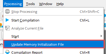
⑥ Update only the initial value data part of the FPGA internal memory by using the following menu in Quartus® Prime.
Processingmenu➤ Update Memory Initialization File
⑦ Using the following menu in Quartus® Prime, a .sof file with updated initial value data for the FPGA internal memory will be generated.
Processingmenu➤ Start➤ Start Assembler
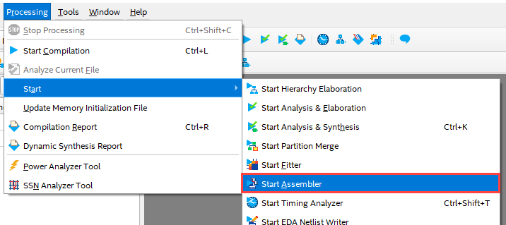
Regenerate the .pof and .jic using the generated (updated) .sof.
▲ Return to the list of work steps
![]() The sample design this time was easy to understand and simple in structure.
The sample design this time was easy to understand and simple in structure.
By further expanding and creating hardware logic circuits and Nios® V systems, a wide range of possibilities open up.
Everyone, please give it a try.
Sample Project
As a sample, we will upload a qar file of a Quartus® Prime project that has performed steps 1 and 2 of this LED blinking design.
Please use this as a reference.
<Notes>
This sample project was created using Quartus® Prime Standard Edition 24.1.
Open niosv_system.qsys in Platform Designer and run Generate HDL before working on it.
▲ Return to the list of work steps
Click here for recommended articles/materials
Getting started with Altera® FPGA
First time blinking LED with Altera® FPGA!
Boot Nios® II with FPGA's on-chip memory
Recommended online seminars and workshops
Get started with Nios® V on an Agilex™ 5 FPGA (see "I want to take the webinar")
Nios® V Processor Introduction Course (see "I want to take training")