- Semiconductor BusinessHOME
- Products and Services of Macnica,Inc.
-
technical information

-
Events and Seminars
- Handling Manufacturer
- Support
- Inquiry
- Click here to purchase products
- Semiconductor business e-mail magazine registration
![]()
![]() Narrow down by specifying conditions
Narrow down by specifying conditions
現在2189件がヒットしています。check

PCI Express in Altera® FPGAs explains how to implement PCI Express in FPGAs. One example is the Avalon Streaming (Avalon-ST) configuration. This section explains how to generate a PCI Express Avalon-ST configuration sample design for Arria® 10.
By using this reference design, you can easily check that the target PC and board environment works. By changing the device model number and pinout, you can also use it to check operation on your own board.
environment
- Tools: Quartus® Prime v17.0
- Development Kit: Arria® 10 GX FPGA Development Kit < Purchase from Macnica-Mouser >
- PC: Desktop PC with PCI Express interface
- OS: Windows® 10
procedure
- Hardware creation
- Install the driver in your desktop PC's OS
- operation check
1. Hardware creation
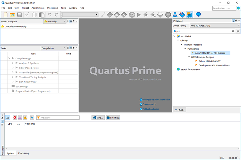
First, launch Quartus® Prime, go to the IP Catalog, set Device Family to Arria® 10, and enter PCI in the search Box.
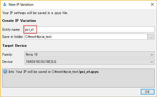
Double-click the Arria® 10 Hard IP for PCI Express to launch Qsys. A New IP Variation will appear, so enter an appropriate Entity Name. Here, I used pci_st.
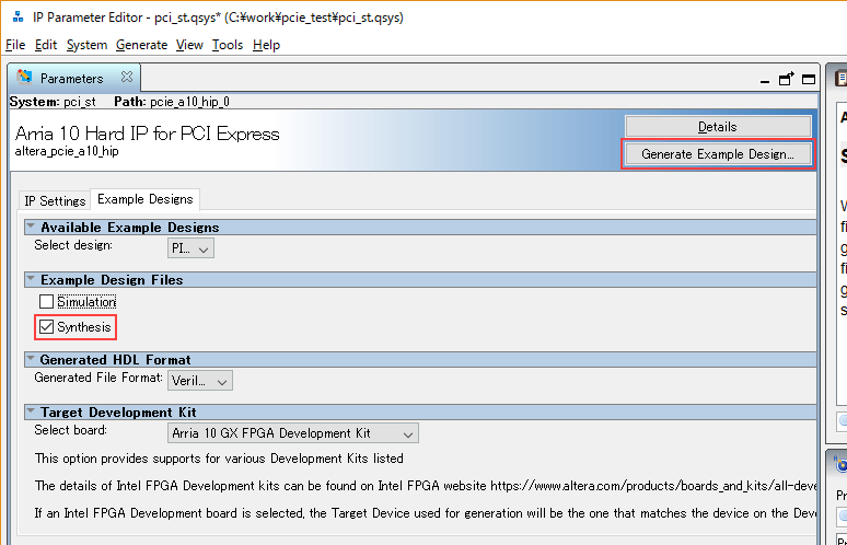
Click the OK button to save the Qsys file. The Qsys screen looks like this: Since we are going to generate an example design, select the Example Design tab. To check the operation on the actual device, check Synthesis and click the Generate Example Design button.
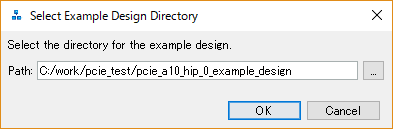
You will be prompted for a location to save the file, so specify the folder where you want to save the file and click the OK button.
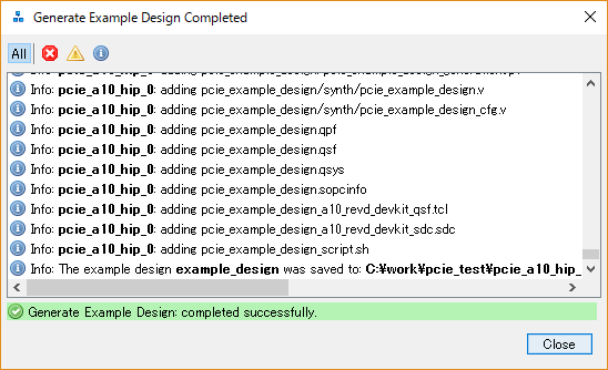
A sample design is generated.
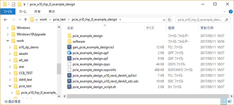
The contents of the generated folder are as follows.
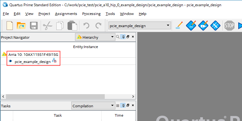
Open the generated project by selecting pcie_example_design.qpf from the Quartus® Prime File menu ⇒ Open Project. The Arria® 10 GX Development Kit device is pre-configured.
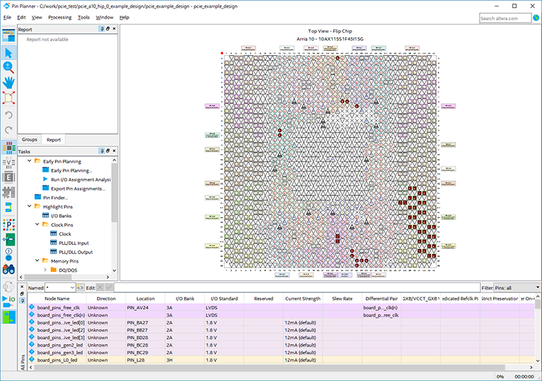
If you open the Quartus® Prime Pin Planner, you will see that the necessary pin assignments have already been made.
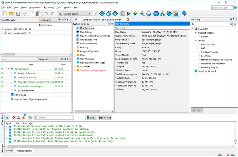
Compile the design. When the compilation is complete, it will look like this: Timing constraint files must also be created manually. At this point, the timing has not been met, but we will continue.
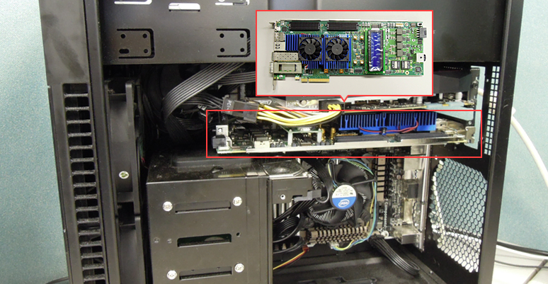
Insert the evaluation board into your PC and power it on.
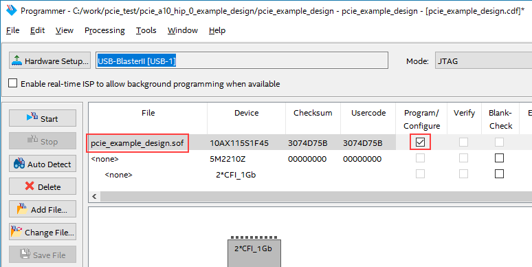
Connect the JTAG cable (USB cable) and write the generated SOF file. Once the burning is complete, restart your PC. Note that you will be restarting your PC here. By restarting, the PCI Express design written by the PC system is correctly recognized and the PC is restarted.
2. Install the driver in your desktop PC's OS
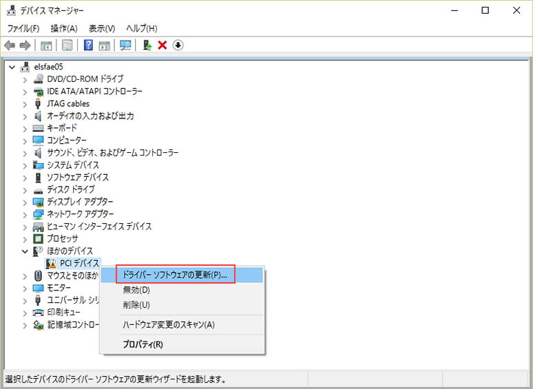
After the PC boots, launch Device Manager. As shown in the figure below, an unknown PCI device is recognized, so update the driver/software.
Run (R) Browse my computer for driver saltware.
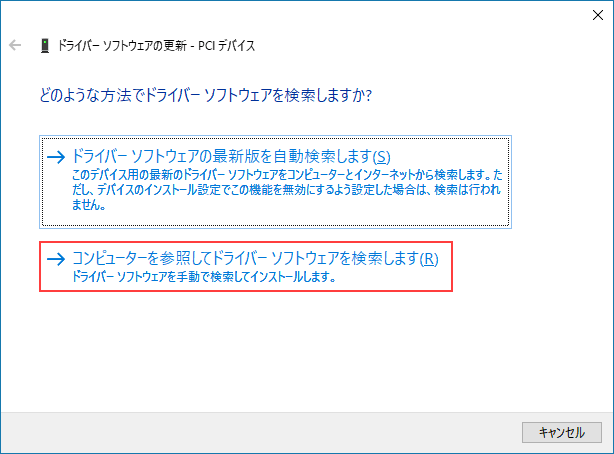
Specify the location of the driver software. The Altera®_PCIe_Interrop_Test.zip is located in the following path in the generated sample design folder, so please unzip it beforehand.
pcie_a10_hip_0_example_design\software\windows\interop
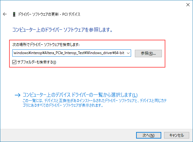
After unzipping, specify the following folder as the driver reference location.
pcie_a10_hip_0_example_design\software\windows\interop\Altera_PCIe_Interop_Test\Windows_driver\64-bit
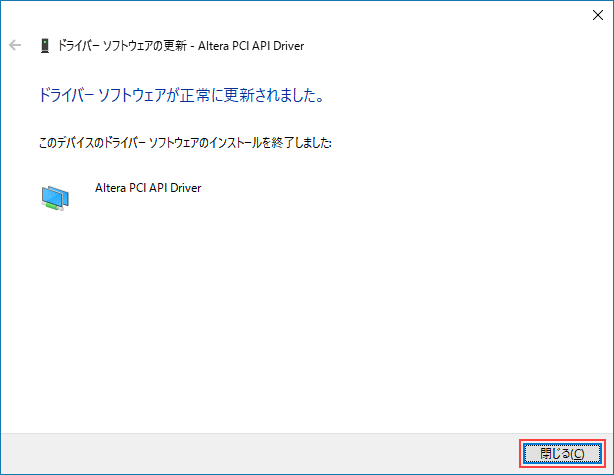
Click Next to install the driver software. Close the screen with Close.
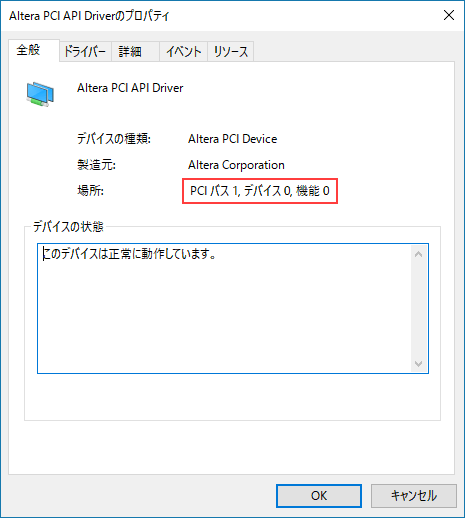
Confirm that it is correctly recognized on the device manager.
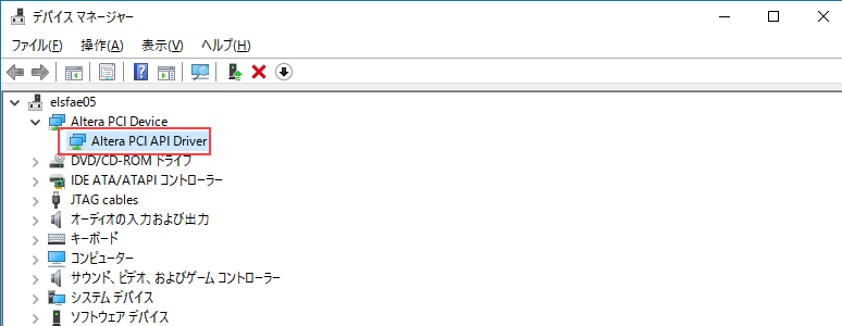
Open the properties of the Altera® PCI API Driver and check the bus number, device number, and function number.
3. Operation check
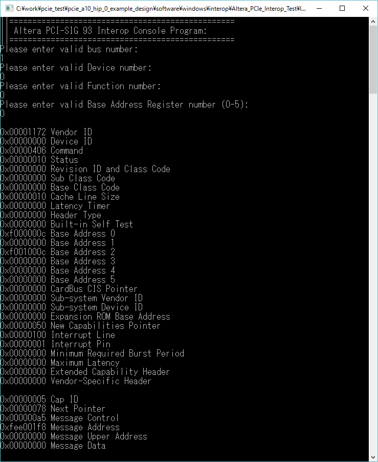
Double-click Alt_Test.exe in the folder below to start it.
pcie_a10_hip_0_example_design\software\windows\interop\Altera_PCIe_Interop_Test\Interop_software
You will be asked to enter the bus number, device number, and function number, so enter the values you checked in advance. Next, you will be asked to specify the Base Address Register Number, so specify 0 here.
If it can be accessed correctly, it will read and display the PCI register information in the FPGA as shown below.
Looking at the log below, you can see Gen3 (=Lane Rate: 3) and x8 (=Link Width: 08).
Also, when PASSED! is displayed at the end, it means that simple data writing, reading, and verifying have completed successfully.
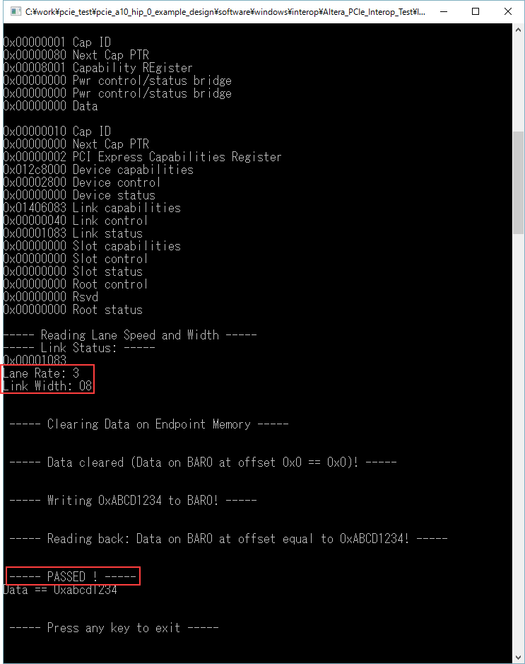
Since we were able to verify access via Base Address 0, we were able to confirm that we had basic access.
User guide
Arria® 10 / Cyclone® 10 GX (Avalon-ST)
https://www.intel.com/content/dam/www/programmable/us/en/pdfs/literature/ug/ug_a10_pcie_avst.pdf
Stratix® V (Avalon-ST)
https://www.intel.com/content/dam/www/programmable/us/en/pdfs/literature/ug/ug_s5_pcie_avst.pdf
Arria® V (Avalon-ST)
https://www.intel.com/content/dam/www/programmable/us/en/pdfs/literature/ug/ug_a5_pcie_avst.pdf
Cyclone® V (Avalon-ST)
https://www.intel.com/content/dam/www/programmable/us/en/pdfs/literature/ug/ug_c5_pcie_avst.pdf
Stratix® IV / Arria® II / Cyclone® IV
https://www.intel.com/content/dam/www/programmable/us/en/pdfs/literature/ug/ug_pci_express.pdf
Click here for recommended articles/materials
PCI Express with Altera® FPGAs
PCI Express with Altera® FPGA (Avalon-MM Edition)
FPGA PCI Express Design & Debug Guidelines
Altera® FPGA Development Flow / Top Page