- Semiconductor BusinessHOME
- Products and Services of Macnica,Inc.
-
technical information

-
Events and Seminars
- Handling Manufacturer
- Support
- Inquiry
- Click here to purchase products
- Semiconductor business e-mail magazine registration
![]()
![]() Narrow down by specifying conditions
Narrow down by specifying conditions
現在2179件がヒットしています。check

This series uses reference circuits for evaluation boards for converter ICs to explain important characteristics in selecting various discrete components.
When explaining, use LTspice for individual characteristics, change the constants of the parts or the parts themselves, check the changes on the circuit with simulation waveforms and calculated values, and explain the relationship between the characteristics and the circuit. Masu.
This time, we will explain how to select the MOS-FETs necessary for DC/DC converter circuits, while confirming the effects of MOS-FET characteristics using simulations. This time as well, we will divide the explanation into two parts, the first part and the second part.
Also, please refer to the following for LTspice and evaluation kits used in the explanation.
[How to download / use LTspice]
・ LTspice download page (link to Analog Devices website)
*If you want to know how to use LTspice, please check the Company article below.
table of contents
・ Introduction: Types of MOS-FETs
・ Role of MOS-FETs in Power Circuits
・ Voltage, current rating
Part 2
・Gate-source voltage: VGS
・ON resistance between drain and source: RDS(ON)
・Total gate charge: Qg characteristics
Introduction: Types of MOS-FETs
MOS-FET is an English acronym that combines Metal Oxide Semiconductor and Field Effect Transistor. Although it can be used as an analog element like an analog amplifier, it is used as a switching element in a switching power supply circuit.
There are two types of MOS-FETs: N-channel MOS-FETs and P-channel MOS-FETs.
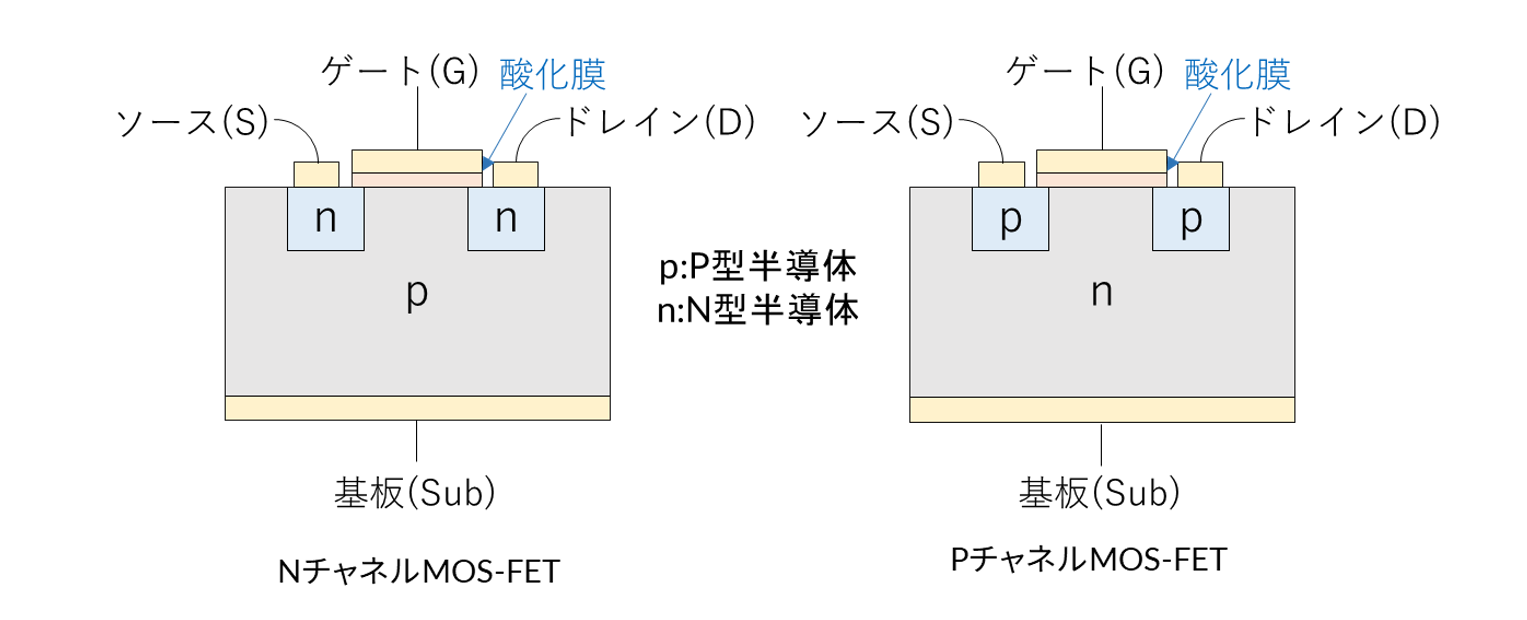
An N-channel MOS-FET turns on when a positive voltage is applied to the gate with respect to the source, and a P-channel MOS-FET turns on when a negative voltage is applied to the gate with respect to the source.
Both N-channel MOS-FETs and P-channel MOS-FETs are used in power supply circuits. Therefore, N-channel MOS-FETs are often used.
It is further classified into enhancement (normally off) type and depression (normally on) type. The enhancement type allows a current to flow when a gate voltage is applied, and the depletion type allows a certain amount of current to flow even when the gate has a negative voltage.
In this article, we will use the enhancement type of N-channel MOS-FET as the material for explanation.
1. Role of MOS-FETs in Power Circuits
In the asynchronous buck converter explained in Part 1 of this series, the diode performs rectification to supply current to the output side while the high-side switch is off. In other words, the diode acts as a low-side switch.
However, at that time, the forward voltage (VF) of the diode becomes a loss and affects the efficiency of the power supply circuit. Losses also occur during switching when the diode is turned on and off. After turning off, the current flows in the opposite direction by a certain amount. The greater the current, the greater the loss. (See Part 1 of this series for details.)
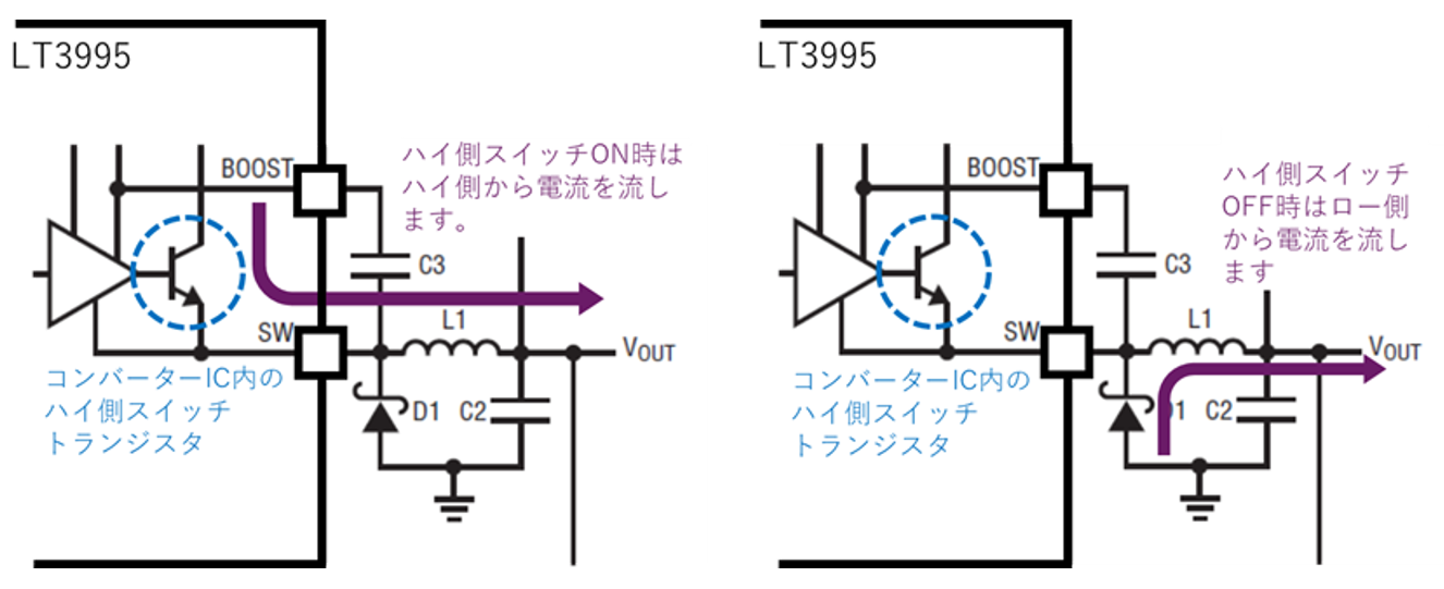
Diagram of "1. Role of diode and effect on converter IC" (reprinted)
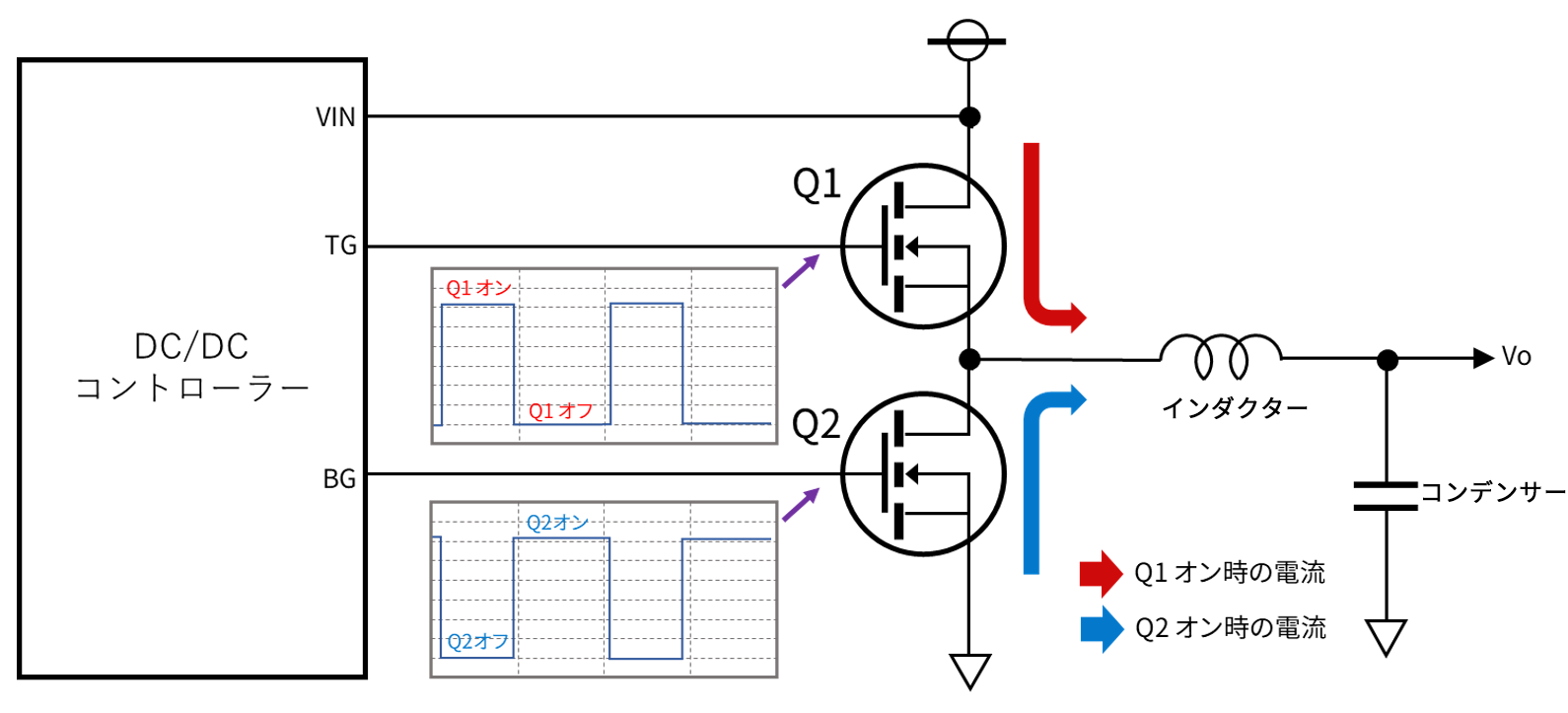
Using power MOS-FETs with low on-resistance instead of diodes, and also using MOS-FETs with low on-resistance as high-side switches, and synchronizing the two power MOS-FETs so that they turn on and off alternately. can realize a low loss converter.
In the figure below, when the Q1 MOS-FET is on, the Q2 MOS-FET is off. Also, when Q1 is off, Q2 turns on, alternately supplying current between Q1 and Q2.
If Q1 and Q2 operate synchronously so that they are not turned on at the same time, a low-loss current switching circuit can be realized.
When using a MOS-FET as a switching element, it is necessary to carefully consider the characteristics of the MOS-FET when selecting the element. The characteristics that are important in this regard are:
"point"
- Using a MOS-FET enables low-loss current switching.
- The important characteristics when selecting a MOS-FET are as follows.
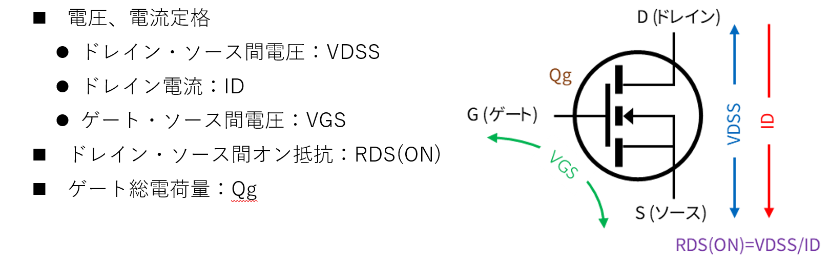
2. Voltage, current rating
The maximum permissible values such as the current that can flow in a power MOS-FET, the voltage that can be applied, and power loss are specified as maximum rated values.
If the maximum rating is not taken into account when designing the circuit, the power MOS-FET will not operate effectively, but will be damaged, shortening its life, or in the worst case, destroying the MOS-FET.
It is very important to observe the maximum rated values in order to operate reliably enough for the target operating time.
The main items specified as rated values are "drain current", "voltage between terminals", "power loss", "junction temperature", and "storage temperature". A power MOS-FET must be selected so as not to exceed the value.
Also, since these characteristics are closely related to each other, they should be considered comprehensively rather than as individual characteristics.
(1) Drain-source voltage: VDSS
This is the maximum voltage that can be applied between the drain and source when the gate and source are shorted.
If a voltage exceeding the rating is applied, it may enter the breakdown region and damage the MOS-FET, resulting in a loss of reliability. In the worst case, the MOS-FET will be destroyed.
(2) Drain current: ID
The maximum DC current that can flow continuously between the drain and source.
ID is limited by power loss due to drain-source on-resistance. Therefore, it is also affected by heat radiation conditions, and the junction temperature must be set to a current value that does not exceed the rated value, and must be used at or below that current value. In addition to the loss limit, it is also limited by the current carrying capability of the package, maximum junction temperature and safe operating area.
(3) Gate-source voltage: VGS
This is the maximum voltage that can be applied between the gate and source.
The rating is based on the withstand voltage of the gate oxide film. It is defined in consideration of practical voltage and reliability.
(4) Power dissipation: PD
Maximum allowable power loss. During ideal switching operation, no current flows when the MOS-FET is off, and no voltage is applied when it is on, so theoretically no power loss (voltage x current) occurs.
However, in actual cases, an on-resistance exists between the drain and source when on, causing loss.
Even if the on-resistance is as low as several tens of mΩ or less, it cannot be overlooked if a large current flows.
Also, if the gate voltage does not sufficiently exceed the threshold voltage, the half-on resistance will increase.
In addition, loss can also be caused by intermediate states of current and voltage during switching transitions.
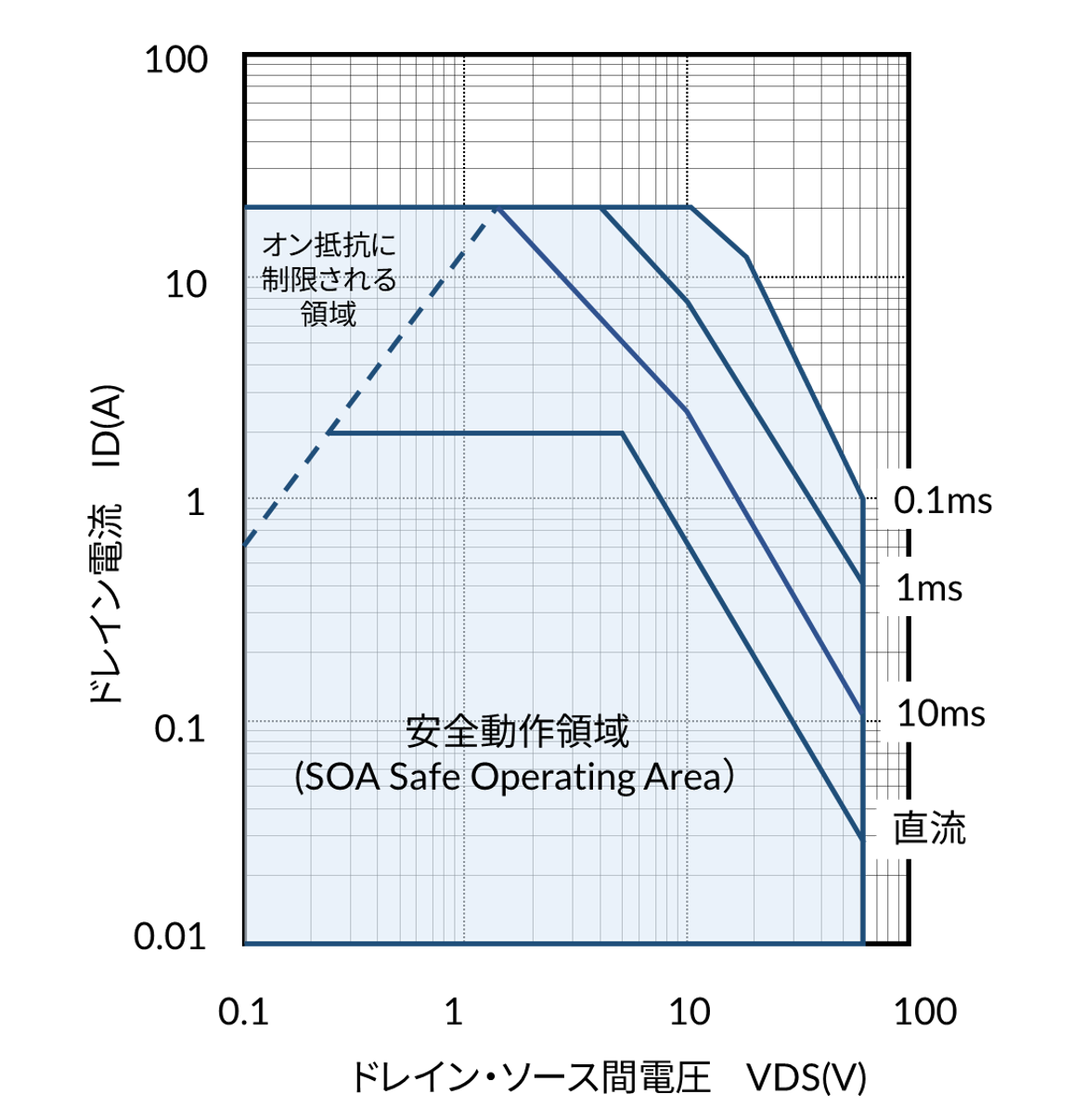
Among these characteristics, there is a regulation called Safe Operating Area (SOA) for voltage and current characteristics. SOA is sometimes called ASO (Area of Safe Operating).
The horizontal axis of SOA is the drain-source voltage (VDS) of the MOS-FET, and the vertical axis is the drain current ID. Both the horizontal and vertical axes are logarithmic.
Most MOS-FET datasheets have an SOA as shown below.
In this figure, the light blue area is the SOA, that is, the area where MOS-FETs can operate safely.
"point"
- Select so that the following rated values are not exceeded on the circuit used.
■ Drain-source voltage: VDSS
■ Drain current: ID
■ Gate-source voltage: VGS
■ Power dissipation: PD
2. Voltage and current characteristics are stipulated as Safe Operating Area (SOA), and should be used within that range.
Improve your circuit design skills by understanding the characteristics of discrete components!
In recent years, the design period has become tight due to the early introduction of products to the market. Even with proven designs and reference designs, discrete components must be selected for circuit optimization. At that time, this technical article will tell you the selection method that will be your base.