- Semiconductor BusinessHOME
- Products and Services of Macnica,Inc.
-
technical information

-
Events and Seminars
- Handling Manufacturer
- Support
- Inquiry
- Click here to purchase products
- Semiconductor business e-mail magazine registration
![]()
![]() Narrow down by specifying conditions
Narrow down by specifying conditions
現在2182件がヒットしています。check

Hello. I'm Tonpa, a new FAE.
I joined Macnica as a new graduate and learned about circuit design and implementation while experiencing manufacturing through production training. When I was a student, I majored in organic chemistry, and since I started with no knowledge of electricity and electronics, I often struggled.
Therefore, in this article, I will introduce what I learned about circuit design and implementation while experiencing manufacturing through manufacturing training. Last time, we introduced the selection of DC/DC converters, but this time we will introduce the board design of DC/DC converters.
Introduction
After deciding on the parts to use, I finally began the board design process.
Before actually designing, I thought it wouldn't be that difficult, but I realized how difficult the design was because there were so many things to worry about.
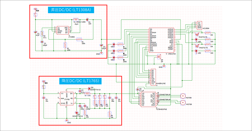
I created a circuit diagram based on the recommended circuit diagram in the data sheet and thought, ``Okay, all that's left to do is implement this.'' However, my senior colleague taught me that we also need to consider the layout when mounting on a board. I started thinking that layout was just about connecting parts on a board, but that wasn't the case at all.
From here, I will introduce what I learned when thinking about board layout.
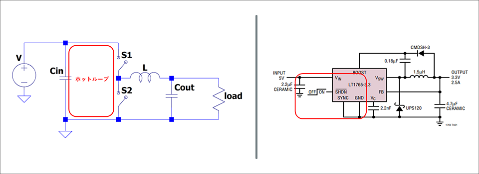
hot loop
When considering the layout of a DC/DC converter, you need to be careful about hot loops. A hot loop is a part where current flows discontinuously due to switching, and it has a large effect on the generation of EMI noise in DC/DC converters.
The hot loop of a step-down DC/DC converter is the part surrounded by the red frame in Figure 2.
So how should we be aware of hot loops?
The key is to make the hot loop as small as possible (shorten the wiring). Longer wiring increases parasitic inductance and generates more EMI noise. For ICs with built-in switching elements like the one shown in Figure 2 (right), the placement of the input capacitor is important, so be sure to place it as close as possible to the IC's input pins and connect it with the thickest wiring possible.
Additionally, the location of the hot loop is different in boost DC/DC converters (red frame in Figure 3). Therefore, in the case of a step-up DC/DC converter, care must be taken when placing the output capacitor.
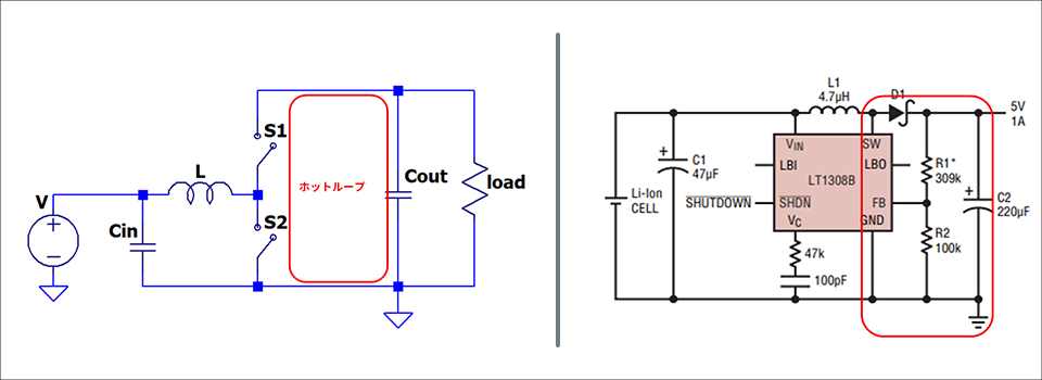
Of course, other parts placement and wiring are also important, but what I paid the most attention to was the hot loop layout. By the way, it took me more than two days to complete the layout.
GND
How to connect GND is very important in board design, regardless of whether it is a DC/DC converter or not. Since GND serves as the voltage reference for the circuit, it is necessary to design a stable GND.
Now, I would like to introduce three things that I paid attention to when designing the GND.
1. Wide GND plane
After all, it is desirable to make the GND as wide as possible in order to stabilize the potential. In my case, it was difficult to have a wide GND plane around the parts, so I designed it with a large GND plane in one part of the board.
2. Connect all GNDs
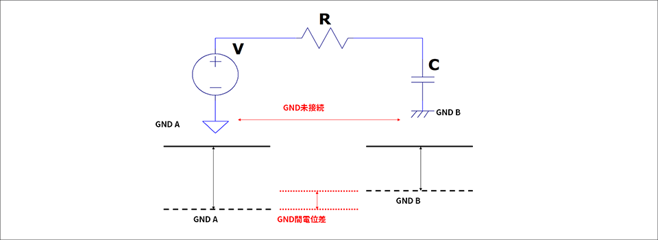
When designing, you will likely have multiple GNDs, but all of these GNDs need to be unified somewhere. As I mentioned earlier, GND serves as the reference for the voltage within the circuit, so all GNDs within the circuit must be at the same potential. If the GNDs are not connected and there is a potential difference between them, the voltage will be different even for the same signal.
3. GND separation
Earlier I told you to connect all the GNDs, and now I want to separate them? Some people may think so. Don't worry, even though they are separated, they will ultimately be connected to one GND. In the case of a printed circuit board, the first layer separates the power GND and signal GND, and the second layer connects them to a common GND.
To put it simply, why it is necessary to separate GND is to suppress the negative effects of noise. The current in the circuit is constant and does not flow, and noise is generated as a voltage due to the changing current and the resistance component in the circuit. If GND is shared, noise generated in one circuit may flow in and adversely affect other circuits. In particular, if the power system GND, which carries a large current, and the detection system GND are common, noise from the large current may flow into the control circuit and cause malfunction.
Therefore, the GND of circuits that are sensitive to noise or have large current fluctuations may need to be separated. Noise can also be reduced by making the wiring connected to GND as short and thick as possible. I don't think it's an exaggeration to say that how to arrange GND is the most important and difficult part of board design.
On our homepage, there is an article focusing on power GND and signal GND, so please refer to this as well.
PCB layout for handling high switching frequencies in regulators (3)
Summary
This time, I introduced hot loops and GND, which I learned while designing a DC/DC converter board. I thought that board design only consisted of creating a circuit diagram, but I was able to learn the importance of thinking about the layout.
The next part will be about mounting the board. Please look forward to seeing what kind of board it will be.
The path to my first circuit design Article list
・DC/DC converter board design
・ Implementation of DC/DC converter
・ Bonus