- Semiconductor BusinessHOME
- Products and Services of Macnica,Inc.
-
technical information

-
Events and Seminars
- Handling Manufacturer
- Support
- Inquiry
- Click here to purchase products
- Semiconductor business e-mail magazine registration
![]()
![]() Narrow down by specifying conditions
Narrow down by specifying conditions
現在2136件がヒットしています。check
Recent Altera® FPGAs naturally support external memory interfaces (EMIF) such as DDRx. By the way, Altera® FPGA people call EMIF "e-mi-fu."
What is the first thing that comes to mind when you think about implementing a memory controller in an Altera® FPGA?
- What FPGA devices does it support?
- What memory standards does it support?
- What transfer rate does it support?
I'm sure you have many questions, such as:
This page is for those who are implementing EMIF with Altera® FPGA for the first time, and explains the process from selection to operation confirmation using a DDRx SDRAM controller as an example.
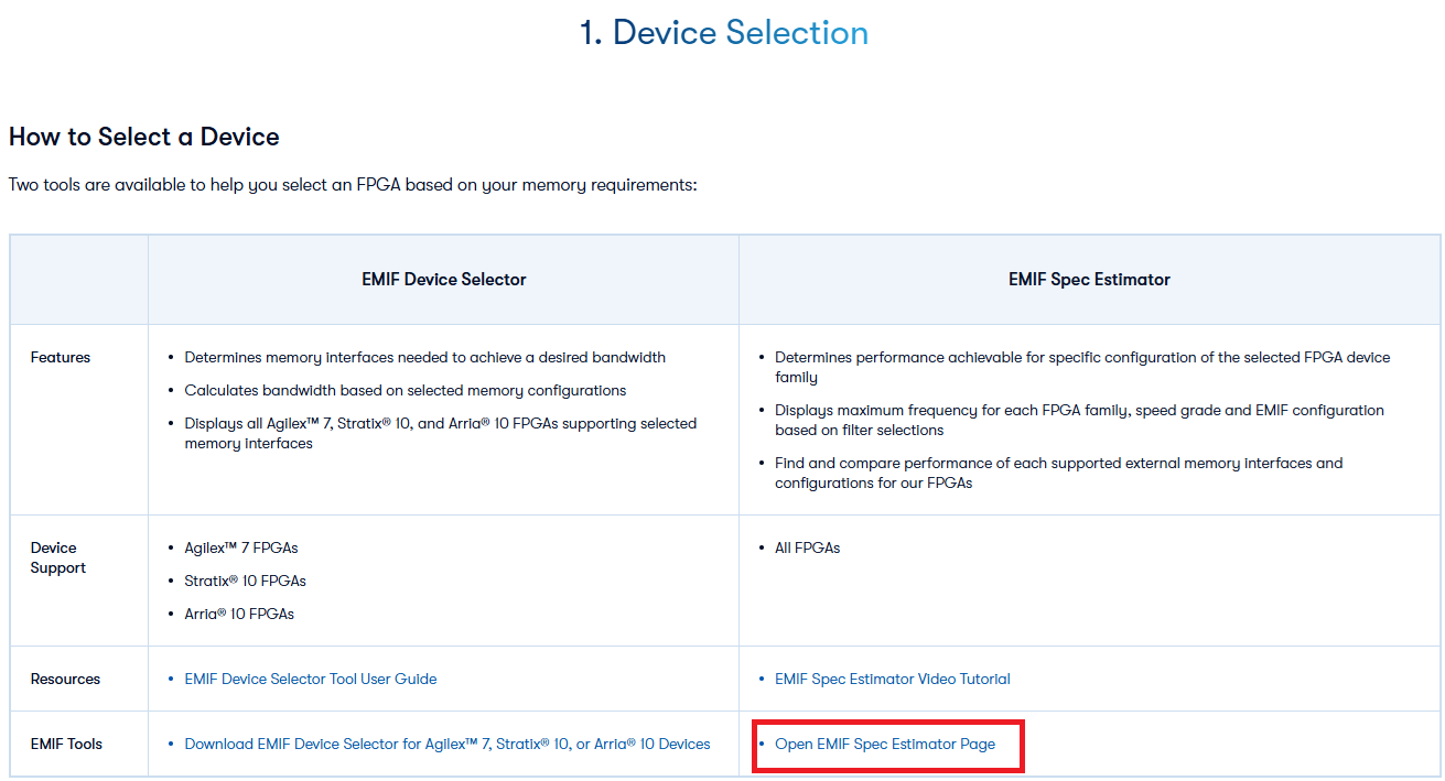
Checking EMIF Support Status
Here is a useful page to check the EMIF support status of Altera® FPGAs.
- External Memory Interfaces IP Support Center (Altera® website)
This page links to the External Memory Interface (EMIF) Spec Estimator, which you can use to check EMIF support in Altera® FPGAs.
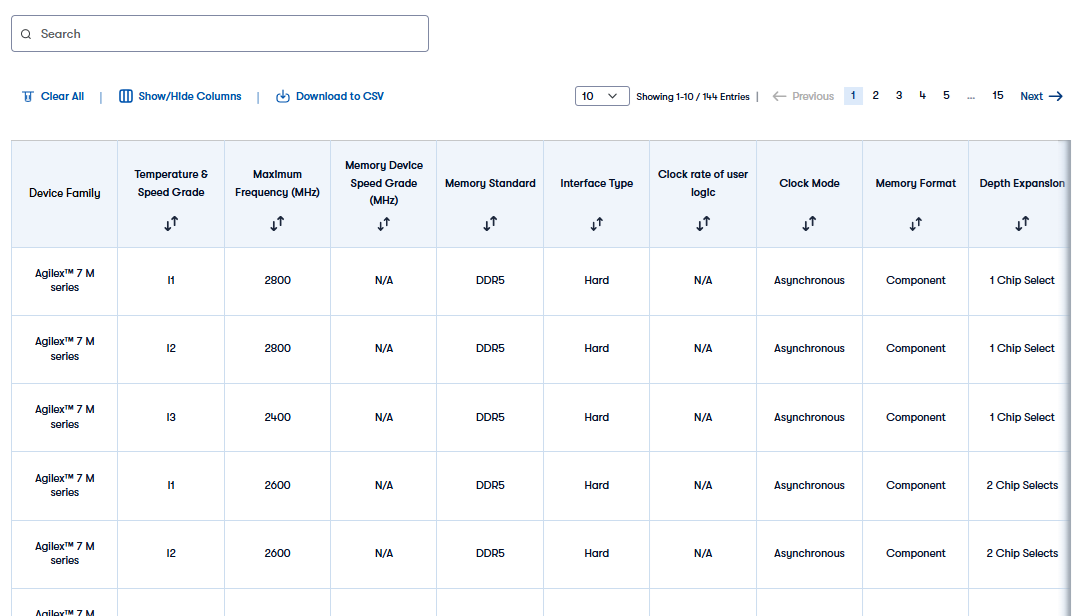
You can search by various criteria, such as device family, speed grade, interface type, memory standard, and frequency.
First, click on the Open EMIF Spec Estimator Page (see below) in the External Memory Interfaces IP Support Center.
The External Memory Interface (EMIF) Spec Estimator (see below) will be displayed, allowing you to select (narrow) various conditions.
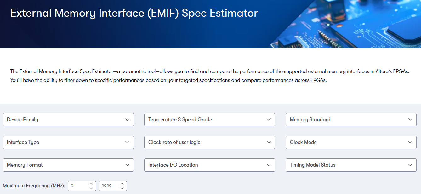
Device Family
Check the device families you want to use or are considering. You can check multiple device families.
If none are checked, all device families will be included.
Temperature Range & Speed Grade
Check the temperature range and speed grade of the device.
<Temperature range>
The following temperature ranges exist. However, depending on the device, there are temperature ranges that exist and temperature ranges that do not exist, so please refer to the documentation of each device for details.
- Commercial temperature range (C product): Junction temperature 0 to 85°C
- Industrial temperature range (I product): Junction temperature -40 to 100°C
- Automotive temperature range (A product): Junction temperature -40 to 125°C
- Extended temperature range (E product): Junction temperature 0 to 100°C
- Military temperature range (M product): Junction temperature -55 to 125°C
<Speed Grade>
Each device family determines the speed grades available, please refer to the device documentation for more information.
Interface Type
- soft
The memory controller is implemented by consuming FPGA resources such as logic and internal memory, often referred to as a soft memory controller (SMC).
- hard
It uses a memory controller that is already hardened inside the device, often called a hard memory controller (HMC).
- Hard HPS
It uses the memory controller built into the hard processor system (HPS) of the SoC FPGA with integrated ARM* cores.
Memory Standards
Select the external memory standard.
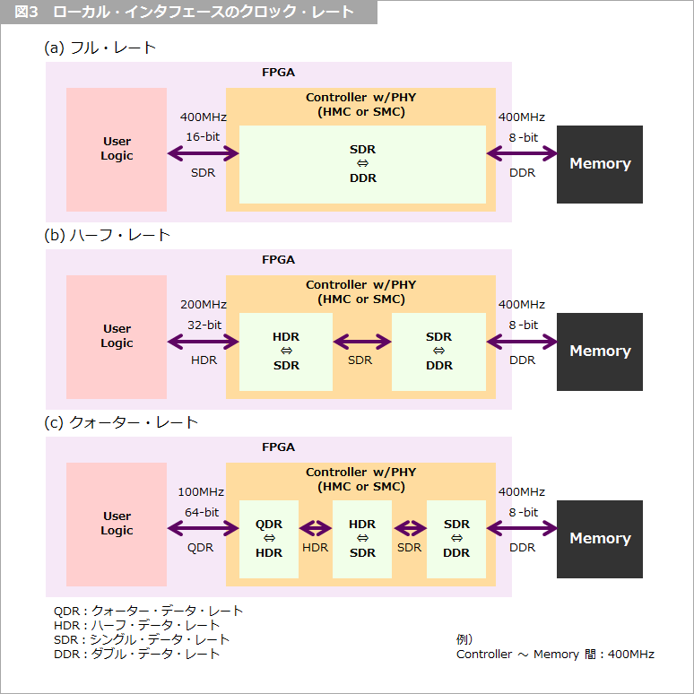
Local interface (User Logic) clock rate
If there is a preference, please select it.
The image is as shown in the figure below. (To make it easier to understand, we're using a double data rate of 400MHz (800Mbps) between the controller and memory.)
Simply put, data is transmitted between the controller and memory at high speed and double data rate, but inside the FPGA, the data cannot be processed at double data rate, so it is first converted to single data rate at the same frequency. However, at this time, the data width is doubled. This is full rate.
Next, if the frequency is too high for the FPGA to process the data at full rate, the frequency is halved again, but this time the data width is doubled again. This is half rate.
Furthermore, if the frequency is too high for the FPGA to process the data at half rate, the frequency is halved again, but the data width doubles again, resulting in quarter rate.
Memory Format
This item selects the memory topology, which can be a component (memory device) or a module (e.g., DIMM).
Interface I/O Location
This item specifies which FPGA bank the EMIF-related pins are placed in. Some FPGAs support different transfer rates depending on the I/O bank location.
Timing Model Status
Select the timing model compatibility.
Maximum frequency (MHz)
Specifies the upper and lower limits of the memory interface (between the memory controller and memory) frequency.
search results
Click "Confirm conditions and search" to display results that meet the specified conditions. Even after the results are displayed, you can further specify conditions to narrow down your search.
From these results, you can check the FPGA candidates to use for the external memory interface, so please consider other interfaces and conditions when deciding which FPGA to use.
Practice
In this practical session, we will introduce how to generate and simulate a memory controller to be implemented in an Altera® FPGA, and how to check its operation using a development kit.
DDR4
DDR3
Design & Debug Guidelines
As the speed of the external memory interface (EMIF) increases, issues such as a shrinking data valid window and deterioration of signal quality have been raised.
As the time spent on verification and debugging to meet required specifications is increasing, it is important to design device boards using appropriate procedures and to implement debugging measures in advance at the design stage.
This document shows the design flow and debug flow, and is intended to help you solve problems quickly by following the appropriate design procedures to prevent defects from being introduced and by implementing the mechanisms required for debugging.
EMIF Design & Debug Guidelines for FPGAs
Click here for recommended articles/materials
DDR3 operation on Altera® FPGA! (Practical Edition) [1/2]
DDR3 operation on Altera® FPGA! (Practical Edition) [2/2]
DDR4 operation on Altera® FPGA! (Practical Edition)
EMIF Design & Debug Guidelines for FPGAs
Altera® FPGA Development Flow / Top Page