- Semiconductor BusinessHOME
- Products and Services of Macnica,Inc.
-
technical information

-
Events and Seminars
- Handling Manufacturer
- Support
- Inquiry
- Click here to purchase products
- Semiconductor business e-mail magazine registration
Product Summary
Certus-NX is a next-generation Lattice FPGA platform, an ultra-low-power general-purpose FPGA constructed with a 28 nm FD-SOI process that consumes far less power per operating frequency than conventional FPGAs. .
Product hardware and features
FD-SOI
Features of FD-SOI
・28nm process
・Overwhelmingly low power consumption per operating frequency (up to 1/4 power consumption compared to devices of the same scale band and operating frequency)
- More than 100 times more soft-error resistance than conventional products
PCI Express
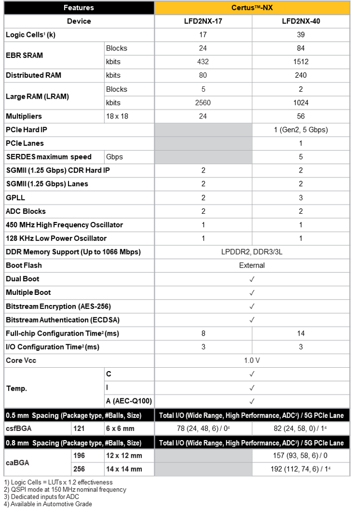
Certus-NX has a built-in PCI-Express (Gen1, Ge2) hard block, making it possible to support interfaces in a wider range of fields than ever before.
Supports MIPI I/F
Realization of MIPII/F with programmable I/O and logic
・Supports data rate of 1.5Gbps per lane
・When configured with CLK 1lane and Data 4lane, one Soft MIPI D-PHY block supports data rates up to 6.0Gbps
・Supports both MIPI CSI-2 and MIPI-DSI
Enables a wide range of I/F bridges on the camera interface side and display interface side.
LRAM
Certus-NX has a large memory block called LRAM separate from EBR. With a maximum capacity of 2560 kbit, it is possible to handle cases where a certain amount of memory capacity is required, such as configuring a line buffer without using an external memory.
ADC
It has 2 channels of 1 MSPS, 12-bit SAR ADC. This allows analog signal processing from sensors, monitoring of supply voltages, etc.
Other components
Programmable I/O
・It is possible to support various I/F such as MIPI, LVDS (Rx, Tx), Sub-LVDS (Rx), HiSPI (Rx), SLVS200 (Rx, Tx), LVCMOS, etc.
・Supports data rates up to 1.5Gbps/lane when using differential I/F
I2C, SPI hard block
・Built-in I2C and SPI hard blocks. Can be configured via I2C, SPI
・Configurable from the host CPU and SoC using these hard blocks without external FLASH (several tens of ms with Quad SPI)
・Quad SPI is also supported, enabling configuration in the order of tens of milliseconds.
DSP block
・Built-in up to 56 18 X 18 Multipliers
DRAM interface
・Compatible with DRAM I/F (supports DDR3, DDR3L, LPDDR2, LPDDR3, up to 1066 Mbps)
Example of product use
The figure below is just an example, so please feel free to contact us from the inquiry button at the bottom of this page regarding the feasibility.
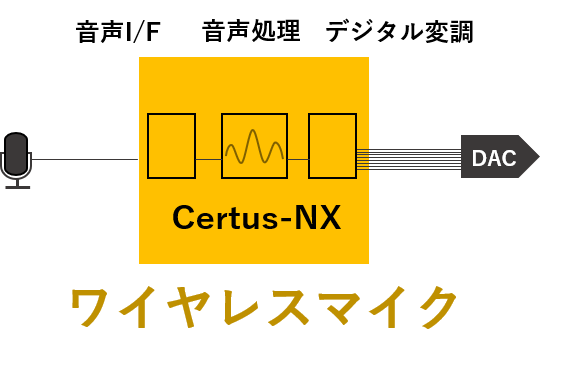
Usage example 1
Example of use with a battery-powered wireless microphone
・Audio I/F
・Audio processing (filters, etc.)
・Digital modulation processing
・DAC I/F
・ Ultra low power consumption
Package lineup
Inquiry / Quotation
If you have any questions or requests for quotations regarding this product, please contact us using the form below.
Design Tool Information
The design tool for Certus-NX is "Radiant".
Click here for Lattice FPGA product information
Related Information
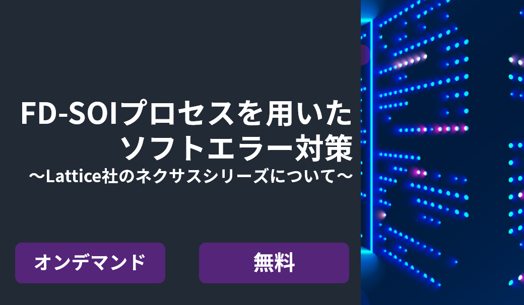
This is an on-demand seminar that you can watch as many times as you like at your convenience.
Soft error countermeasures in Lattice's Nexus series using the FD-SOI process will be explained through details of the FD-SOI process and an actual SED/SEC demonstration.