- Semiconductor BusinessHOME
- Products and Services of Macnica,Inc.
-
technical information

-
Events and Seminars
- Handling Manufacturer
- Support
- Inquiry
- Click here to purchase products
- Semiconductor business e-mail magazine registration
![]()
![]() Narrow down by specifying conditions
Narrow down by specifying conditions
現在2183件がヒットしています。check

The edge artificial intelligence (AI) chipset market is expected to surpass the cloud AI chipset market for the first time in 2025.
ABI Research, a consulting firm in the global technology market, estimated that the cloud AI chipset market had US$11.9 billion in revenue that year, while
We estimate that the edge AI chipset market will reach US$12.2 billion.
Edge AI includes smartphones, wearable devices, smart cars, and smart homes/industries/cities.
Among them, the smart home will be a major driver of the edge AI market.
Most AI training workloads occur in public and private clouds.
Centralizing these workloads in the cloud has traditionally provided benefits of flexibility and scalability.
However, the need for privacy, cybersecurity, and low latency make it more desirable to run it in gateways, devices, and sensors.
Recent advances in key areas, such as new AI learning architectures and high-performance computing chipsets, have played a key role in this shift.
Edge AI computes data as close as possible to physical systems. This has the advantage that data processing does not require a network connection.
Data calculations are done near the edge of the network where the data is formed, rather than in a central data processing center.
The biggest benefit of edge AI is the ability to ensure real-time results for time-sensitive needs.
Under various circumstances, sensor data can be collected, analyzed and communicated instantly, without the need to send data to a time-sensitive cloud center.
In addition to being used in smartphones, deep learning is also used in IoT devices, and recently it is called AI and IoT combination, or AIoT.
Edge AI brings new concepts to legacy IoT, but the computing power of traditional IoT processing units, MCUs, is too weak to perform deep learning.
Currently, there are two types of hardwired mechanisms that assist these MCUs. It's a DSP or dedicated accelerator (called a deep neural network, DNN).
These hardwired mechanisms can be implemented as IP or chips.
The basic building blocks of the main DNN algorithms, convolutional layers and fully connected layers, are both multiply-accumulate (MAC) operations.
A high degree of parallelism is heavily used to achieve high performance.
Many iterations of weights stored in DRAM are updated according to different training styles.
Regardless of the mechanisms described above, DRAM throughput is key in DNNs.
Therefore, choosing a suitable DRAM is very important for AIoT applications. Unlike cloud environments, low power consumption is a concern in edge computing,
AIoT device planners need to balance performance and power savings.
In addition to power consumption and performance, the capacity required for the DRAM installed in AIoT devices will be lower (1-2 Gbits) than the DRAM (8-16 Gbits) for mobile phones and PCs.
Winbond Electronics' 1Gbit LPDDR3 DRAM is one example, which AI company Kneron has used in its latest system-on-chip (SoC), the KL720.
The KL720 is one of the company's SoCs used in a variety of edge devices such as battery-powered applications such as smart locks and drones.
LPDDR3 provides a maximum bandwidth of 8.5GByte/s with dual 1.2V/1.8V power supplies.
This enables customer devices such as Kneron's KL720 to process 4K, full HD, 3D sensor video images in real time to support AI applications such as face recognition and gesture control for security cameras.
It also enables the execution of natural language processing.
The capacity and bandwidth of Winbond's LPDDR3 DRAM can also be used in automotive applications such as Advanced Driver Assistance Systems (ADAS) employing cameras that need to process video images in real time.
On the other hand, it can be said that there is also a lot of demand for IoT endpoints that require low memory and high bandwidth and are required to perform basic AI inference.
As shown in Figure 1, LPDDR4/4x provides approximately double the throughput of LPDDR3, and has similar advantages to LPDDR3 over LPDDR2.
Regarding the IO voltage, the IO voltage of LPDDR4 is 1.1V, while LPDDR4x is 0.6V, contributing to lower power consumption as well as improved transfer rates.
JEDEC has already released the latest LPDDR5 standard, but the capacity of LPDDR5, which has just entered the market, is still too large for AIoT applications.
For now, LPDDR4x is still the best choice if you need more AI compute power than LPDDR3 can provide.
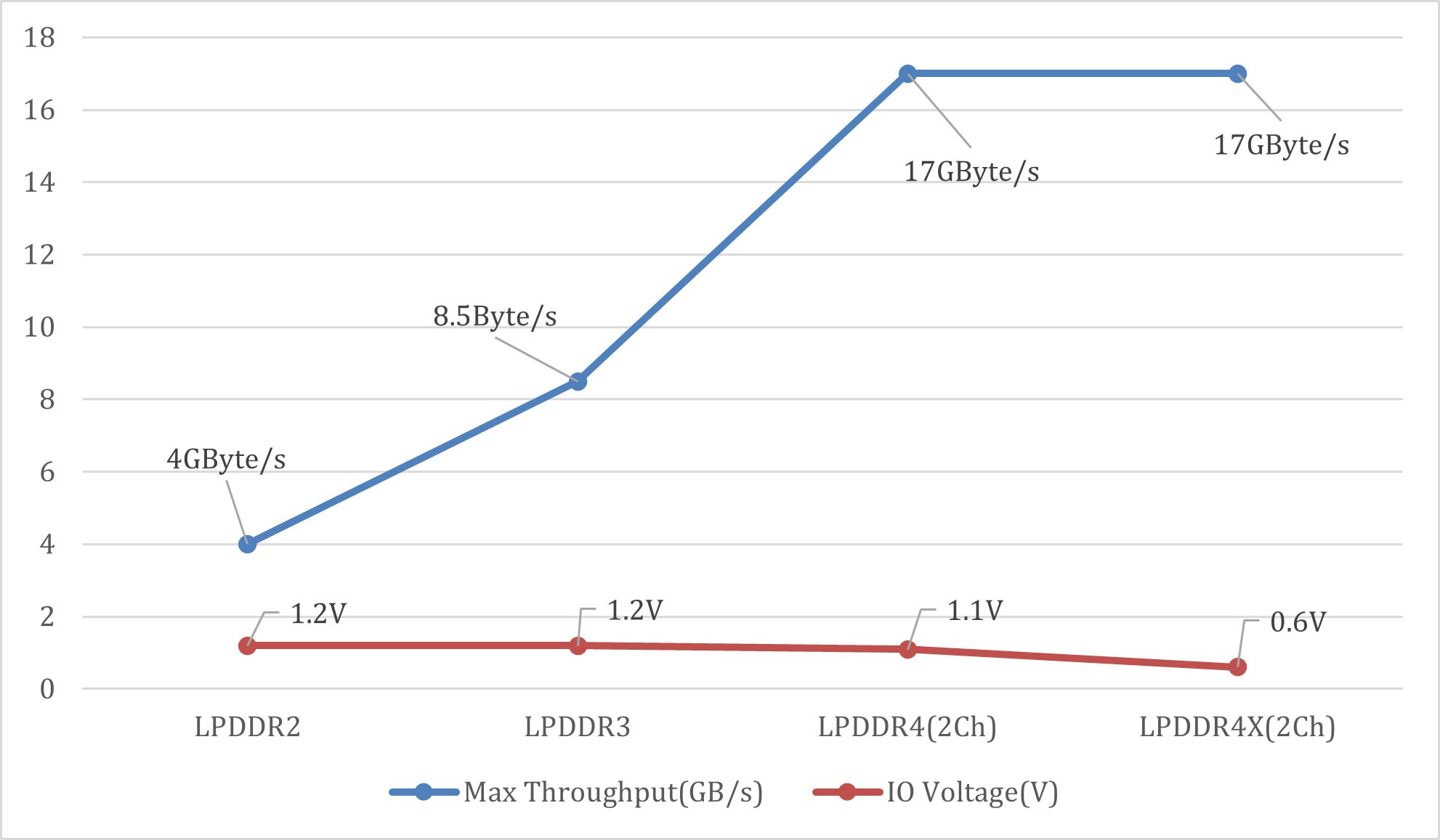
Figure 1
Winbond owns its own wafer fab and ranks among the top four IC manufacturers offering both DRAM and NOR/NAND Flash.
Winbond's LPDDR4/4x DRAM series ranges in capacity from 1 to 8Gbit, adopts the self-developed 25nm technology node, and achieves speeds up to 4266Mbps.
In addition to KGD (known good die), standard 200BGA package is also available.
Click here for related links
Inquiry / Quotation
If you have any questions about this product, request a sample, or request a quote, please contact us using the form below.
Back to Winbond Manufacturer Information Top
If you want to return to Winbond manufacturer information top page, please click below.