- Semiconductor BusinessHOME
- Products and Services of Macnica,Inc.
-
technical information

-
Events and Seminars
- Handling Manufacturer
- Support
- Inquiry
- Click here to purchase products
- Semiconductor business e-mail magazine registration


 Narrow down by specifying conditions
現在2247件がヒットしています。check

When creating a circuit board for implementing Altera® FPGAs, designers create the circuit diagram by referring to the documentation published by the manufacturer.
Here, we will guide you to the points that you should pay special attention to.
It should be noted that Q
Target FPGA
・ Cyclone® V
Advance preparation
Here are some documents that can be used as reference when creating circuit diagrams.
|
Pin connection guidelines |
Schematic review worksheet |
| Cyclone® V Device Family Pin Connection Guidelines | Cyclone® V Device Schematic Review Worksheet |
Cyclone® V Overview (FPGA TOP)
The diagram below shows the pins that require special attention in the PCB design for Cyclone® V.
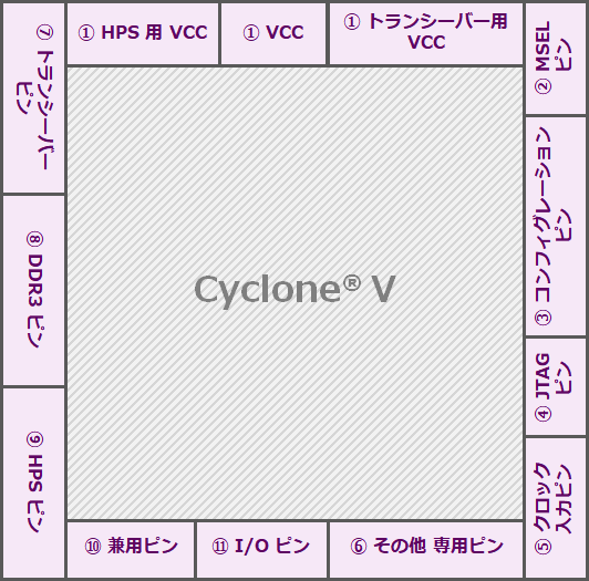
* The layout in the diagram has nothing to do with the actual device.
Click each item to see the check points.
| ① VCC, VCC for HPS, VCC for transceiver | ② MSEL pin | ③ Configuration pin |
| ④ JTAG pins | ⑤ Clock input pin | ⑥ Other dedicated pins |
| ⑦ Transceiver Pins | ⑧ DDR3 pin | ⑨ HPS pin |
| ⑩ Dual-purpose pin | ⑪ I/O pins |
― |
① VCC, VCC for HPS, VCC for transceiver
|
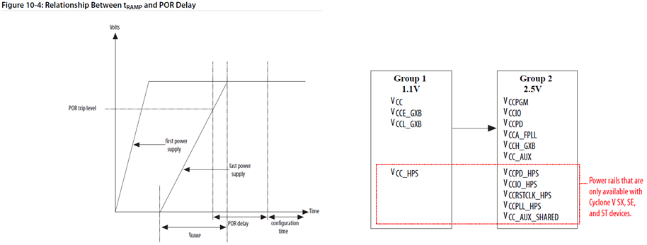
● Refer to the datasheet and apply the recommended power supply voltage. |
|
● Establish a measurement point near the FPGA ・Be ready to measure the power supply in case of trouble |
|
● Refer to Power & Thermal Design & Debugging Guidelines |
|
● When not using all GXBs (transceivers) on the same side ・VCCE_GXBL and VCCL_GXBL can be connected to GND |
|
● Number of decoupling capacitors ・Estimate with reference to the PDN tool ・For a more detailed estimate, use a dedicated tool <Reference> Power Delivery Network (PDN) Analysis Tool Part 9 Confirmation and Review of Capacity in FPGA Power Supply Design |
|
● When configuring in Active Serial (AS) mode ・ VCCPGM is 3.0 V or 3.3 V |
|
● Power sequence For more details, please refer to this document (Power-Up Sequence Recommendation for Cyclone® V Devices). |
② MSEL pin
Please see below for MSEL pin information for Cyclone® V.
|
MSEL Pin Settings |
Inserting pull-up/pull-down resistors(1)(2) |
| Cyclone® V |
(see linked documentation) |
(1) A Weak Pull-Down Resistor (25kΩ) is inserted inside.
(2) If you want to switch the configuration mode, please switch to VCCPGM/GND with a 0Ω resistor.
See here for a list of MSEL pins.
③ Configuration pin
|
● DCLK ・Recommend inserting damping resistor (minimum 0Ω) 10-50Ω - In AS mode, take care of the trace length (see the document below) "Evaluating Data Setup and Hold Timing Slack in AS Configuration" |
|
● nCONFIG, nSTATUS ・Pull up to VCCPGM via 10kΩ resistor |
|
● CONF_DONE ・Pull up to VCCPGM via 10kΩ resistor ・Do not connect to the LED as it is. - Due to lack of drive current, it may not light up without applying FET |
|
● When FPGA is cascaded, nSTATUS and CONF_DONE are common and pulled up. - INIT_DONE is pulled up individually (only if used) |
|
● nCE ・Pull down via GND connection or 10kΩ resistor ・This signal determines whether the FPGA is cascaded. |
|
● When using nCEO, pull up to VCCPGM through a 10kΩ resistor. |
④ JTAG pins
|
● Check Point ・It is recommended to insert a 0Ω damping resistor for TCK. - To support cases where writing is not possible due to problems with the clock system |
|
● Pin processing ・TCK: Pull down via 1kΩ resistor (Pull down via 1kΩ resistor even when not used) ・TDI: Pulled up to VCCPD via 1kΩ to 10kΩ resistor (pulled up via 1kΩ resistor when not used) ・TMS: Pulled up to VCCPD via 1kΩ to 10kΩ resistor (pulled up via 1kΩ resistor when not used) ・TDO : No pull-up/pull-down (open when not used) |
| ● When cascading three or more FPGAs, insert buffers on the TCK and TMS lines. |
⑤ Clock input pin
|
● Assign to p-channel when using single-ended clock (This is a limitation when using the ALTCLKCTRL buffer because n-channel does not directly ride on the global clock.) |
|
● Pay attention to AC/DC coupling when inputting differentially |
|
● Pull down the RREF_TL pin through a 2kΩ resistor when using the PLL (resistor accuracy is ±1%) |
⑥ Other dedicated pins
|
pin name |
comment |
| RREF_TL |
Pulled down through a 2kΩ±1% resistor |
| VREF | Connect to VCCIO or GND if not used as a dedicated pin |
⑦ Transceiver Pins
|
● Connect to GND when transceiver is not used. ・Connect the clock (REFCLK_*) to GND ・RX (GXB_RX_*, GXB_REFCLK_*) is connected to GND ・TX (GXB_TX_*) is floating |
|
● AC/DC coupling ・Adjust to I/O Standard |
⑧ DDR3 pin
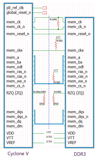
Please refer to the following web content and check according to the guidelines.
• Circuit diagram verification items for Arria® V / Cyclone® V and DDR3 (from Ultima Company technical content)
・ Pins that are particularly easy to mistake
- mem_reset_n
- mem_cke
-rzq
⑨ HPS pin
|
Cyclone® V SoC Pin Names |
comment |
|
CLOCKSEL[1:0] |
Pulled up through a 10 kΩ resistor or pulled down through a 1 kΩ resistor to the VCCIO voltage |
|
BOOTSEL[2:0] |
Pulled up through a 10 kΩ resistor or pulled down through a 1 kΩ resistor to the VCCIO voltage |
|
HPS_nRST (bidirectional pin) |
Pull up to VCCRSTCLK_HPS voltage through 1kΩ to 10kΩ resistor |
|
SDMMC |
Pulled up through a 10kΩ resistor |
| Others |
If you use QSPI > 128Mbit, you need to use an IC with reset (Bootrom software works in 3-byte mode, so you can't boot)
[Reference] Cyclone® V and Arria® V SoC QSPI Boot (from altera-fpga.github.io) |
⑩ Dual-purpose pin
|
pin name |
comment |
|
CLKUSR DEV_OE DEV_CLRn PR_REQUEST |
Connect to GND if not used as a function pin and not used as a user I/O pin. |
| nPERST | Used as reset pin for PCIe hard IP |
⑪ I/O pins
● If you are performing internal calibration, you will need to process the RZQ pin.
Appendix: Cyclone® V MSEL Pin List
MSEL Pin Settings (FPGA Configuration)
|
Device Family |
Configuration Mode |
Compression |
Design Security |
VCCPGM(V) |
POR Delay |
MSEL[4:0] |
|---|---|---|---|---|---|---|
|
Cyclone® V |
FPP x8 |
Disabled |
Disabled |
1.8/2.5/3.0/3.3 |
Fast |
10100 |
| Standard |
11000 |
|||||
|
Disabled |
Enabled |
1.8/2.5/3.0/3.3 |
Fast |
10101 |
||
| Standard |
11001 |
|||||
|
Enabled |
Enabled/Disabled |
1.8/2.5/3.0/3.3 |
Fast |
10110 |
||
| Standard |
11010 |
|||||
|
FPP x16 |
Disabled |
Disabled |
1.8/2.5/3.0/3.3 |
Fast |
00000 |
|
| Standard |
00100 |
|||||
|
Disabled |
Enabled |
1.8/2.5/3.0/3.3 |
Fast |
00001 |
||
| Standard |
00101 |
|||||
|
Enabled |
Enabled/Disabled |
1.8/2.5/3.0/3.3 |
Fast |
00010 |
||
| Standard |
00110 |
|||||
|
PS |
Enabled/Disabled |
Enabled/Disabled |
1.8/2.5/3.0/3.3 |
Fast |
10000 |
|
| Standard |
10001 |
|||||
|
AS(x1,x4) |
Enabled/Disabled |
Enabled/Disabled |
3.0/3.3 |
Fast |
10010 |
|
| Standard |
10011 |
MSEL Pin Settings (HPS Configuration)
|
Device Family |
Configuration Mode |
Compression |
Design Security |
POR Delay |
MSEL[4:0] |
cfgwdth |
cdrratio |
Partial Reconfiguration |
|---|---|---|---|---|---|---|---|---|
| Cyclone® V SoC via HPS |
FPP x16 |
Disabled |
AES Disabled |
Fast |
00000 |
0 |
1 |
○ |
|
Standard |
00100 |
0 |
1 |
○ |
||||
|
Disabled |
AES Enabled |
Fast |
00001 |
0 |
2 |
○ |
||
|
Standard |
00101 |
0 |
2 |
○ |
||||
|
Enabled |
Optional |
Fast |
00010 |
0 |
4 |
○ |
||
|
Standard |
00110 |
0 |
4 |
○ |
||||
|
FPP x32 |
Disabled |
AES Disabled |
Fast |
01000 |
1 |
1 |
× |
|
|
Standard |
01100 |
1 |
1 |
× |
||||
|
Disabled |
AES Enabled |
Fast |
01001 |
1 |
4 |
× |
||
|
Standard |
01101 |
1 |
4 |
× |
||||
|
Enabled |
Optional |
Fast |
01010 |
1 |
8 |
× |
||
|
Standard |
01110 |
1 |
8 |
× |