- Semiconductor BusinessHOME
- Products and Services of Macnica,Inc.
-
technical information

-
Events and Seminars
- Handling Manufacturer
- Support
- Inquiry
- Click here to purchase products
- Semiconductor business e-mail magazine registration


 Narrow down by specifying conditions
現在2240件がヒットしています。check


Hello, I'm Mass Man.
Starting this week, we will be serializing a new project "Timing Analysis Series All 6"!!!
The most difficult part of the new employee training was the lecture on timing analysis. In this column, I would like to summarize the lecture materials and notes on timing analysis and introduce the points where I stumbled.
Fmax (maximum operating frequency)
Timing analysis verifies that the FPGA operates correctly at a certain clock frequency.
The Fmax value is the index for timing analysis. Fmax is the maximum frequency at which the FPGA will operate and is defined in Equation 1. You're calculating if data can get from the transmit register to the receive register in one clock cycle!
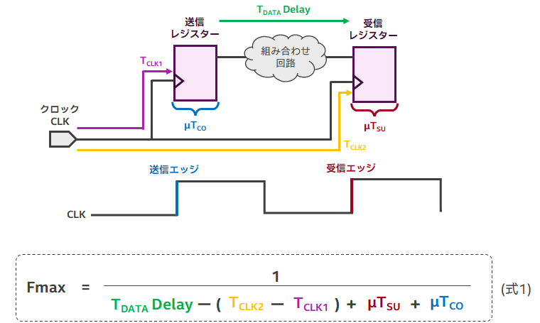
・ T DATA Delay: Data delay time. Depends on circuit design.
・ T CLK2-T CLK1: Clock skew. Wiring dependent.
・ μ TSU: Setup time. The amount of time data must be pre-determined and held relative to the input clock edge of a register. Device specific value.
・ μT CO: Clock to output. Time to data output for register input clock edge. Device specific value.
From Equation 1, we can see that Fmax depends on "circuit design" and "clock skew".
Here, Altera FPGA devices have dedicated routing regions (Global Clock, Regional Clock, etc.) that are aligned to minimize clock skew. When you route the clock signal to Global Clock, the clock skew = 0 (that is, Tclk2 = Tclk1 ), so plugging equation 1 into equation 2.

From Equation 2, Fmax depends on the "circuit design".
Users are required to design so that Fmax is the expected value.
Setup time and hold time
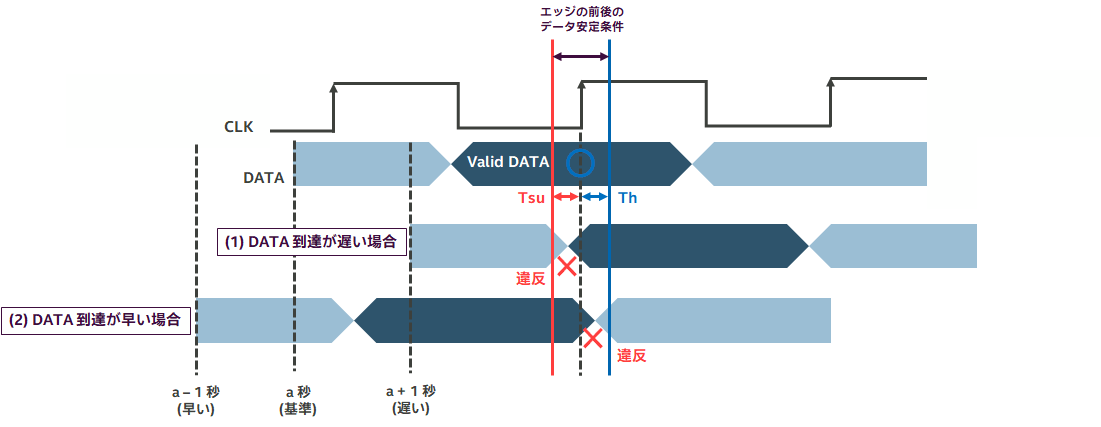
Data must be stable before and after the clock edge to obtain correct data (Figure 2).
Setup Time (Tsu): The time the data (DATA) must be established before the clock edge.
Hold Time (Th): The time the data (DATA) must be held after the clock edge.
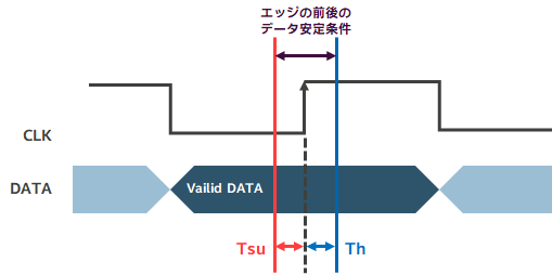
Timing analysis analyzes paths between all registers to ensure setup and hold times are met.
Setup time/hold time violations occur when the timing of the data and the clock edge do not match.
It's sudden, but here's a quiz! !
Based on the clock edge on the left end of Figure 3, which is earlier/later in time, dataA or dataB? ?
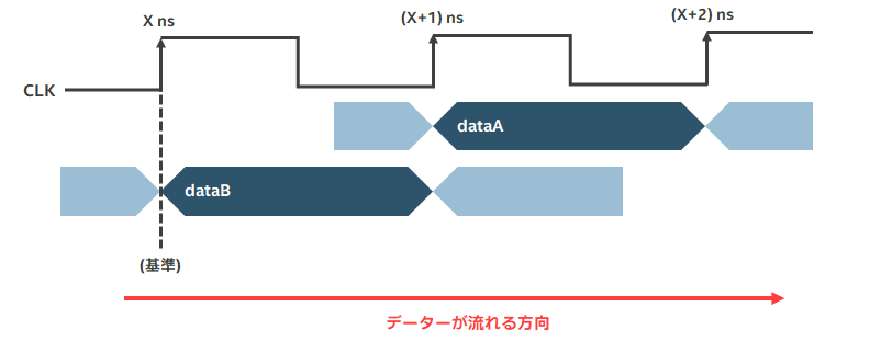
The answer is dataA => slow dataB => fast.
Masuo had the illusion that "dataA is ahead of dataB in the direction of data flow, so dataA is advancing faster in terms of time" (← stumbled point).
However, when representing the behavior of a logic circuit, the time axis is represented from left to right. i.e. relative to the clock edge
The left side is earlier on the time axis
The right side is later on the time axis
It is
I've found that looking at the valid range of data with respect to clock edges is a very important point in understanding timing analysis! !
The upshot is that when the data arrives late with respect to the clock edge, the setup time is violated, and when the data arrives early, the hold time is violated. (Fig.4)
| Summary |
|---|
|
• The Fmax parameter is greatly affected by the “circuit design” (equation 2). |
Next time, I will introduce the SDC file that is absolutely necessary for timing analysis!