- Semiconductor BusinessHOME
- Products and Services of Macnica,Inc.
-
technical information

-
Events and Seminars
- Handling Manufacturer
- Support
- Inquiry
- Click here to purchase products
- Semiconductor business e-mail magazine registration
![]()
![]() Narrow down by specifying conditions
Narrow down by specifying conditions
現在2183件がヒットしています。check


Hello, my name is Taro Washimiya and I work at Macnica providing technical support for Altera® FPGA products.
Recent FPGAs come equipped with a Phase Locked Loop (PLL) as standard, and I believe many users are using the PLL built into their FPGAs.
It's convenient because it allows you to easily generate clocks with different frequencies, but I'm sure there are many users who use it somehow.
Therefore, on this page, I would like to explain basic contents such as architecture, IP generation, etc. from basic principles that can not be heard now.
What should I start with? If you have any doubts, please continue reading this article.
Note that unless otherwise specified, this article covers general-purpose PLLs and does not include PLLs for transceivers.
content
・ PLL location
Clock Network
・ Tips for pin assignment
・ Altera IOPLL
・ Altera PLL
・ ALTPLL
Basic principles of PLL
The basic principle of PLL is roughly shown in the figure below. (The detailed architecture differs depending on the FPGA series and family.)
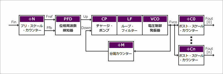
And the table below briefly summarizes each block in the PLL.
| Abbreviation | block name | Explanation |
| PFDs | phase frequency detector | Compare the rising edges of the feedback clock (Ffb) and the input reference clock (Fref). The PFD produces an Up or Down signal that determines whether the VCO should operate at a higher frequency or a lower frequency. |
| CP | charge pump | When the charge pump receives an Up signal, current is driven into the loop filter. When a Down signal is received, current is drawn from the loop filter. |
| LF | loop filter | Converts the Up and Down signals from the PFD to voltages used to bias the VCO. LF also filters glitches from the charge pump to prevent voltage overshoot. This minimizes VCO jitter. |
| VCOs | voltage controlled oscillator | The speed of operation of the VCO is determined by the voltage from the charge pump. A divide counter (M) is inserted in the feedback loop to raise the frequency of the VCO (Fvco) above the input reference frequency (Fref). The VCO frequency is calculated using the following formula: Fvco = Fref * M = Fin * M/N Fin in the equation is the input clock frequency to the PLL and N is the pre-scale counter. VCO frequency is an important parameter and Quartus® Prime automatically sets the VCO frequency within the recommended range based on the clock output and phase shift requirements of the design to ensure proper operation of the PLL. To do. |
| ÷M / ÷N | Division Counter / Pre-Scale Counter | A divide-down counter (÷M) is inserted in the feedback loop to make the VCO frequency (Fvco) higher than the input reference clock. The frequency of the VCO (Fvco) is equal to m times the input reference clock (Fref), and the input reference clock (Fref) is equal to the input clock (Fin) divided by the pre-scale counter (÷N) . |
| ÷Cn | post scale counter | The VCO output can feed multiple post-scale counters (C[n:0]). These post-scale counters allow the PLL to generate a large number of harmonically related frequencies. |
When the reset to the PLL is released, it starts to generate a clock with the set frequency based on the reference clock.
The PFD (Phase Frequency Detector) compares the phase and frequency of Fref and Ffb and continues to output Up / Down signals until they are equal.
When they are equal, a so-called locked state occurs, and a stable clock is output.
(The locked state can be monitored with the locked signal. The locked pin is omitted from the basic principle diagram.)
FPGA architecture
So where is the PLL located in the FPGA?
It depends on the device family.
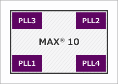
Here we take MAX® 10 as an example.
MAX® 10 has devices with 2 PLLs (PLL1 and PLL2) and 4 PLLs (PLL1 and PLL2, PLL3, PLL4) depending on the lineup and package.
And as shown in the figure, they are mounted on the four corners of the package.
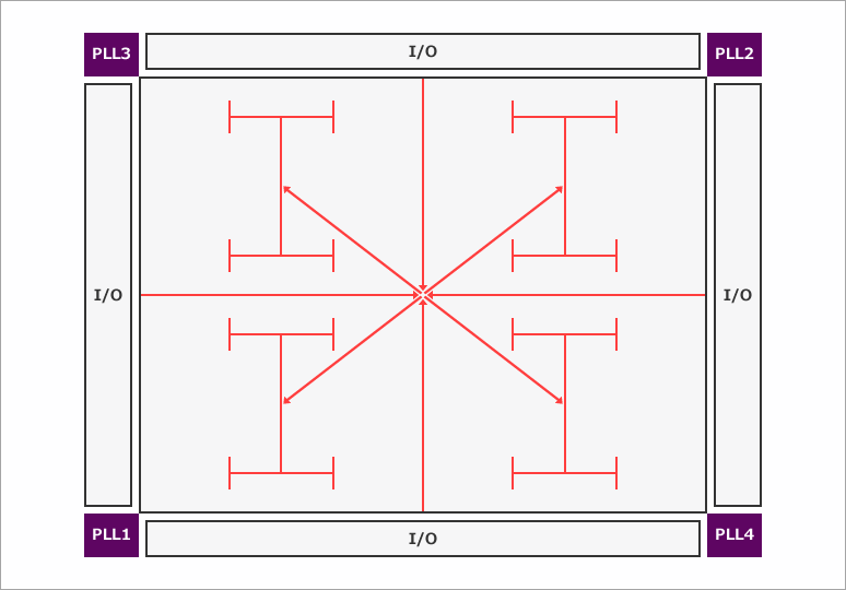
clock network
MAX® 10 has a global clock (GCLK) that runs throughout the device.
This global clock is pre-tuned for low skew, making it ideal for high fanout signals like clocks and resets.
Quartus® Prime automatically assigns high-fanout signals to global clocks at compile time and is usually transparent to the user.
If there are signals that you want to assign to the global clock, you can also constrain them in Quartus® Prime.
In large-scale devices, in addition to global clocks, there are also devices that have regional clocks (RCLK) that are spread within an area that divides the device into four areas.
Clock pin assignment tips
Depending on the device family, there are recommended pins for the input clock (reference clock) to the PLL and pins for outputting the clock generated by the PLL from the FPGA.
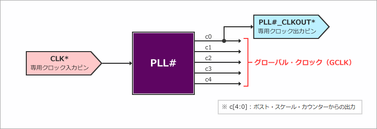
- When using a clock from outside the FPGA as the reference clock for the PLL, it is recommended to use the dedicated clock input pin (Dedicated Clock Pin / CLK*).
- PLL output clocks can be routed to global clocks (GCLK) and dedicated clock output pins inside the FPGA
- If you want to output the clock outside the FPGA, we recommend using the dedicated clock output pin (PLL External Clock Output/PLL#_CLKOUT*).
- PLL location determines which dedicated clock pins are available
More information can be found in the MAX® 10 documentation.
MAX® 10 PLLs and clock networks * See MAX 10 Dedicated Clock Input Pin Connectivity to PLL
MAX® 10-Pin Connection Guidelines
In MAX® 10, c0 output is recommended if you want to output the PLL output clock outside the FPGA.
It is possible to implement it if the compilation passes even if it is other than c0, but it is still recommended to use dedicated wiring.
For other devices, refer to the pin connection guidelines for your target FPGA.
Pin Connection Guidelines
Also, refer to the Altera® FPGA documentation for information on PLLs and clock networks for each device family.
Stratix® series
Stratix® 10 PLLs and Clock Networks
Stratix® V PLLs and Clock Networks (See Clock Networks and PLLs in Stratix V Devices)
Arria® Series
Arria® 10 PLLs and Clock Networks (See Clock Networks and PLLs in Arria 10 Devices)
Arria® V PLLs and clock networks (See Clock Networks and PLLs in Arria V Devices)
Cyclone® Series
PLLs and clock networks in Cyclone® 10 GX devices.
PLLs and clock networks in Cyclone® 10 LP devices. See Clock Networks and PLLs in Cyclone 10 LP Devices.
Cyclone® V PLLs and Clock Networks (See Clock Networks and PLLs in Cyclone V Devices)
Cyclone® IV PLLs and Clock Networks (See Clock Networks and PLLs in Cyclone V Devices)
MAX® Series
MAX® 10 PLLs and Clock Networks
*CPLDs such as MAX® V and MAX® II do not have a PLL.
Generating IP
Different Altera® FPGA device families have different PLL architectures, which means different IP choices.
To implement a PLL in your FPGA design, select the corresponding PLL IP from the Quartus® Prime IP Catalog or the IP Catalog within the Platform Designer system integration tool.
(If you have a Quartus® Prime project open, you can only select the PLL IP that corresponds to your target FPGA.)
| device | Altera IOPLL | Altera PLL | ALT PLL |
| Stratix® 10 | ✔ | ||
| Stratix® V | ✔ | ||
| Arria® 10 | ✔ | ||
| Arria® V | ✔ | ||
| Cyclone® 10GX | ✔ | ||
| Cyclone® 10LP | ✔ | ||
| Cyclone® V | ✔ | ||
| Cyclone® IV | ✔ | ||
| MAX® 10 | ✔ |
I will introduce each PLL setting in another article.
- Altera® FPGA PLL - IOPLL Altera FPGA IP
- Altera® FPGA PLL - PLL Altera FPGA IP
- Altera® FPGA PLL - ALTPLL
Click here for recommended articles/materials
IP-related articles and materials
Altera FPGA Development Flow / Top Page