- Semiconductor BusinessHOME
- Products and Services of Macnica,Inc.
-
technical information

-
Events and Seminars
- Handling Manufacturer
- Support
- Inquiry
- Click here to purchase products
- Semiconductor business e-mail magazine registration


 Narrow down by specifying conditions
現在2247件がヒットしています。check
In "Characteristic Impedance and Driver Drive Capability", we discussed the output resistance of the driver. This time, I will explain how to calculate the optimum value of the damping resistance using this resistance value.
First of all, what is a damping resistor? Damping means to dampen vibration.
Off topic, but a car absorbs shocks from the road surface with springs. However, since the spring alone will cause vibration, a device called a shock absorber is installed to suppress and converge this vibration. This shock absorber is called a damper. In this image, a damper is inserted into the circuit as a component that suppresses and converges the pulse waveform oscillation. I don't know who named it when, but strictly speaking, its main function is not to suppress vibration, but to match the difference between the output resistance of the driver and the characteristic impedance of the line to some extent. Therefore, it might be more correct to call it a matching resistor. However, since no one calls this resistor a matching resistor, we will continue to refer to it as a damping resistor.
As an aside, dumping is another word. Damping resistance values of 22 Ω and 33 Ω are often used. Isn't the reason "somehow" or "because my senior used this value"? Alternatively, insert a zero ohm resistor "for the time being", and after the prototype board is completed, remove the zero ohm resistor in the laboratory. Isn't it a pitiful resistance that can be determined by writing to
The bill of materials is also one of the important blueprints. All numbers written in blueprints have meaning. I think it's pathetic that resistance is decided "for the time being" or "somehow". I want to be able to explain properly when subordinates and juniors ask, "How did you decide this resistance value?" The value of the damping resistor should be chosen to keep the waveform disturbance as small as possible. Take the rising waveform shown in Figure 1 as an example. Please consider the falling edge in the same way.
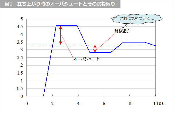
Waveform disturbance is mainly overshoot and its rebound. As long as the overshoot is not very large, I don't think you need to worry about it. If it is too large, it may become a noise source, but it is not a fatal problem, so we will consider the bounce of the overshoot. If this bounce becomes deeper (larger), it will eventually cause corrugation cracks. When the threshold on the Low side is exceeded, it is desirable to select the bounce as small as possible considering the superimposition with other noise. Consider the minimum amplitude margin when the bounce is 25% below full amplitude, or 75% of full amplitude. This level is halfway between the full amplitude (100%) threshold voltage and a typical value of 50%. It is called the minimum amplitude margin in the sense that it should not fall below this level under any circumstances. At this time, the output resistance of the driver is 1/3 of the characteristic impedance of the line. (Footnote 1)
If the characteristic impedance of the line is 50 Ω, the output resistance of the driver is 50 ÷ 3 = 17 Ω. According to "Characteristic Impedance and Driver Drive Capacity", the drive capacity of this driver is 16 mA. For a 70 Ω line, 70 ÷ 3 = 23 Ω for a 12 mA driver. Consider never using these drivers without damping resistors. Actually, it is necessary to lower the drive capacity further, that is, add a damping resistor. Figure 2 is a diagram for determining the damping resistance from the amount of overshoot.
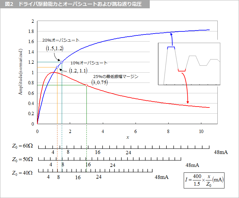
The appropriate amount of overshoot depends on the design concept, but 10% or 20% of full amplitude would be appropriate. For 20% overshoot, x = 1.5, so for a 50 Ω line, 50 ÷ 1.5 = 33 Ω, or an 8 mA driver. Add a damping resistor for drivers with greater drive capability. Figure 3 shows the damping resistor values for a 50 Ω line. a in the figure is the amount of overshoot. If you set it to anything other than 20%, please do your own calculations.
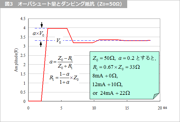
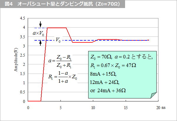
Figure 4 shows the case of a 70 Ω line. It can be seen that a larger damping resistor value is required than for the 50 Ω line. Without looking at the answer at the end of the sentence, try to calculate what the bounce voltage will be at 20% overshoot.
Footnote 1
In the case of ordinary CMOS transmission with only a CMOS receiver at the far end and no termination, if the ratio of the driver's output resistance to the line's characteristic impedance is x, the voltage due to bounced overshoot is: 4x ÷ (1 + x)^2 times the amplitude. Substituting this formula with 0.75 and solving for x, we get x = 3.
answer
Substituting x = 1.5 into the equation in footnote 1 yields 4 × 1.5 ÷ 2.5^2 = 0.96, or only 4% of full amplitude.
What is Yuzo Usui's Specialist Column?
It is a series of columns that start from the basics, include themes that you can't hear anymore, themes for beginners, and also a slightly advanced level, all will be described in as easy-to-understand terms as possible.
Maybe there are other themes that interest you!