- Semiconductor BusinessHOME
- Products and Services of Macnica,Inc.
-
technical information

-
Events and Seminars
- Handling Manufacturer
- Support
- Inquiry
- Click here to purchase products
- Semiconductor business e-mail magazine registration
![]()
![]() Narrow down by specifying conditions
Narrow down by specifying conditions
現在2189件がヒットしています。check

Introduction
After working at a machine manufacturer for three and a half years, working on development work such as housing and mechanism design, I joined Macnica mid-career as an FAE.
Macnica has a large proportion of mid-career employees, so it's very easy to work here and you don't feel alienated at all.
Originally, I studied mechanics at university and had no knowledge of electricity at all when I joined the company, so I started over from Ohm's law and am currently studying desperately.
I had an opportunity to actually design a DC/DC converter under such circumstances, so I hoped it would be helpful for a beginner electrician like myself.
I will introduce the process.
Device used
The first device I designed was the LT8609A from Analog Devices.
There are various types of DC/DC converters, each with a different degree of design difficulty.
・Monolithic Regulator
・Multi-output Regulator
・μModule
・Controller Regulator
The LT8609A is a buck type with only one output per Monolithic Regulator.
The goal is to use this device to create a board that satisfies the following specifications.
・Input voltage : 6~36V
・Output voltage : 5V
・Output current : 2A
·frequency : 2MHz
This time, I will challenge with a universal board instead of a printed board.
Design and parts procurement
First, I determined the constants of each component while looking at the datasheet, and created a circuit diagram using the simulation tool LTspice.
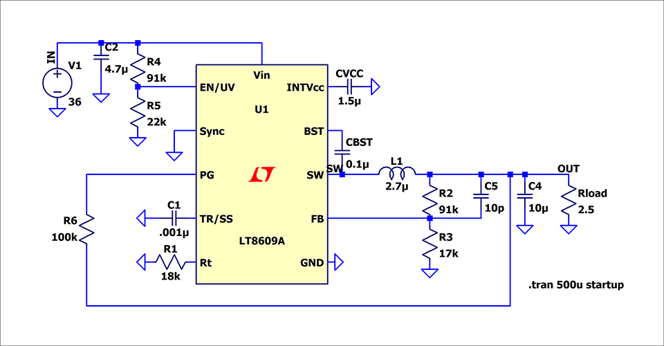
If you create a circuit diagram on LTspice, you can check the operation by simulation as it is
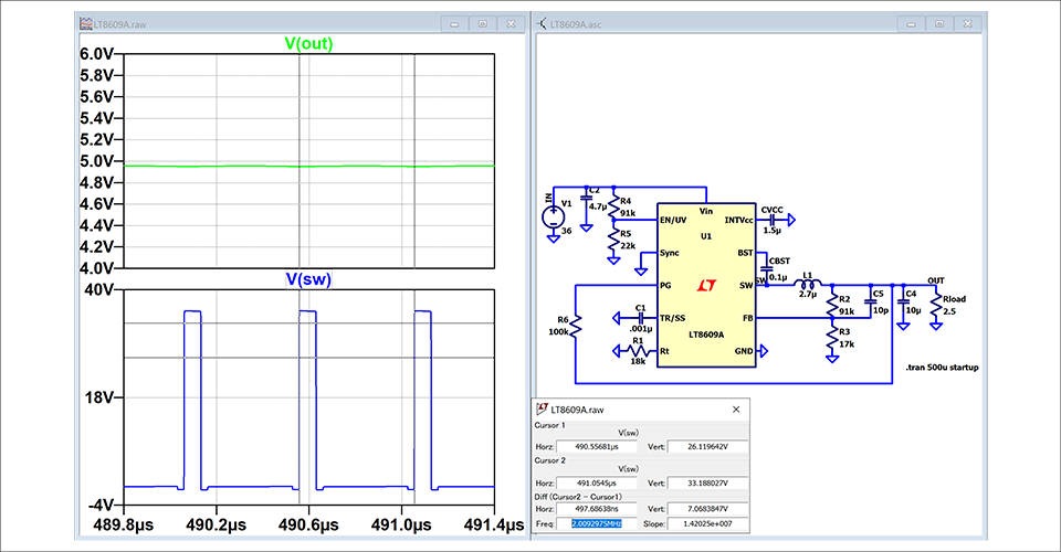
As a result of the simulation, 5V output was confirmed as expected, so the constant seems to be no problem for the time being. When I checked the SW node, I was able to confirm that the switching was properly set to a frequency of 2 MHz.
If you can confirm that it works on the simulation, purchase the parts. This time, we used Mouser and Akizuki Electronic Trading.
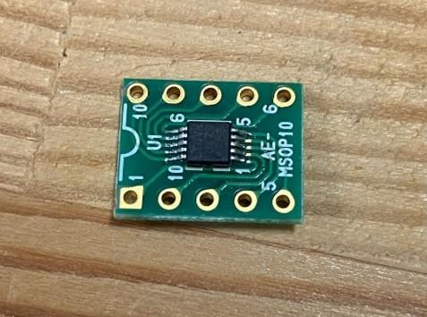
The LT8609A is available in a variety of packages, but the package cannot be mounted directly on a universal board, so I purchased a conversion board from Akizuki Denshi Tsusho.
I bought it from the website linked here.
Component mounting
When the parts arrive, we will implement them.
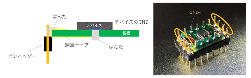
When the LT8609A is mounted on the conversion board purchased from Akizuki Denshi Tsusho, it looks like this.
I was a novice at soldering, so it was quite difficult.
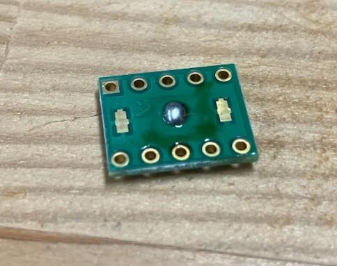
There is also a GND pad on the back side of the device, so turn it over and pour the solder in.
I used a tester to check if the legs of the device and the conversion board were properly connected.
The connection between the conversion board and the main board required some ingenuity.
The problem was the processing of the GND pad on the back side of the conversion board. In order to connect this to the main board, as shown in the cross-sectional view of Figure 5, the conversion board is brought from the back side to the surface with copper foil tape, and shorted to the pin headers glued to both ends.
I thought about connecting the GND by simply pulling it out with a lead wire, but I was told that the stability of the GND is very important for the device, so I decided that this method would be the most reliable.
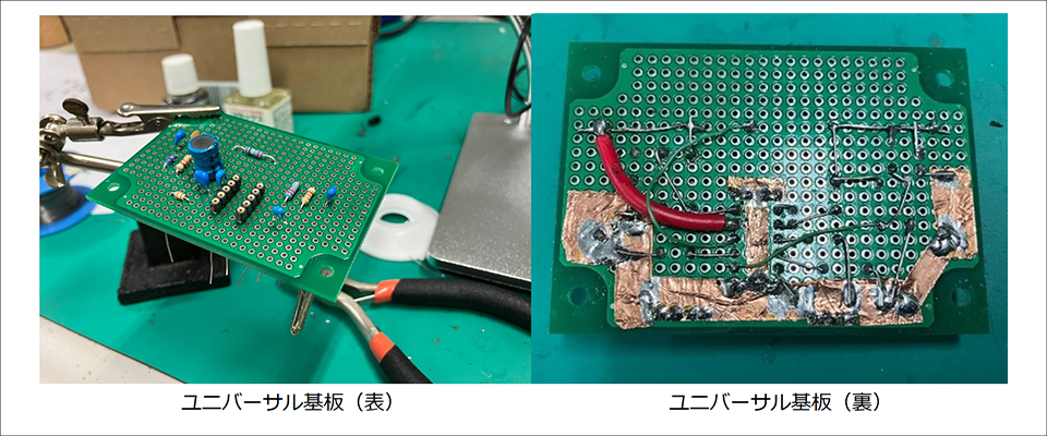
We will mount the purchased parts on the universal board. I've gotten used to handling solder.
In order to mount the device board with the pin header created earlier, mount the pin header-female on the universal board side as well. This way, if your device breaks, you can quickly replace it.
On the back side, I used wires and legs of existing parts to wire. Assemble the wiring of the part where the current flows while observing the rule that it is thick and short (this is quite difficult). As for the GND, I was advised to "strengthen it as much as possible", so I used copper foil tape to secure a large GND area.
That's it for this time.
I didn't have any knowledge of electricity, so it was my first time to handle everything from arranging parts to designing and mounting on my own.
Coming from a background in mechanical design, I used to have a bad image of electrical wiring, but in reality, I was bound by various restrictions, and I was able to experience firsthand that the world's printed circuit boards are things that have been thoroughly thought out. I was. I realized once again that I need to accumulate as much experience as possible and become more powerful in order to support customers in electrical design.
Next time will be "Purification".
We will actually move the board we created this time. Please look forward to whether it will work.
Universal board edition article list
■Universal board edition
・I tried making a DC/DC converter using a universal board (1)
・ I tried making a DC/DC converter using a universal board (2)
・ I tried making a DC/DC converter using a universal board (3)
・ I made a DC/DC converter using a universal board (4)
■Printed circuit board edition
・ Create a power supply with your own printed circuit board! (1)
・ Create a power supply with your own printed circuit board! (2)
・ Create a power supply using a homemade printed circuit board! (3)
・ Create a power supply using a homemade printed circuit board! (4)
・ Create a power supply using a homemade printed circuit board! (5)