- Semiconductor BusinessHOME
- Products and Services of Macnica,Inc.
-
technical information

-
Events and Seminars
- Handling Manufacturer
- Support
- Inquiry
- Click here to purchase products
- Semiconductor business e-mail magazine registration
![]()
![]() Narrow down by specifying conditions
Narrow down by specifying conditions
現在2189件がヒットしています。check

Have you ever wondered whether the switching frequency of a DC/DC converter should be kept high or low?
Not long ago, 300 to 500 kHz was the mainstream, but recently products with a switching frequency of 1 to 2 MHz have become common, and there are even products with a switching frequency of 4MHz or higher.
For high-frequency DC/DC converters, it is possible to reduce the size of the inductors used, enabling the miniaturization of power supply circuits. This is a must-have feature for small portable products. However, it is well known that increasing the switching frequency has the disadvantage of reducing efficiency.
In this article, we briefly discuss ideal and real-world circuit simulations, review switching waveforms, and see the effects of PCB layout.
This time, for the first time, I would like to use an ideal simulation model to confirm that small parts can be used when the switching frequency of the regulator is high.
Constant setting of inductor and output capacitor
Here, we will create an ideal circuit using LTspice and check its operation.
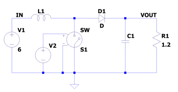
Using the circuit shown in Figure 1, configure a boost converter with an input voltage of 6 (V), an output voltage of 12 (V), and a load current of 10 (A).
Using this ideal circuit,calculate the constants of the inductor and output capacitor used when the switching frequency is 2MHz and 400kHz, and compare how much the values change. After that, check if the same characteristics can be obtained when the circuit is operated with the calculated constants.
Inductor selection
Calculate the inductor value. Since the duty ratio is required to calculate the inductor, it is calculated as shown in formula 1.
Vo : Output voltage
VIN : Input voltage
VD : Diode forward voltage
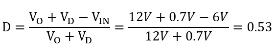
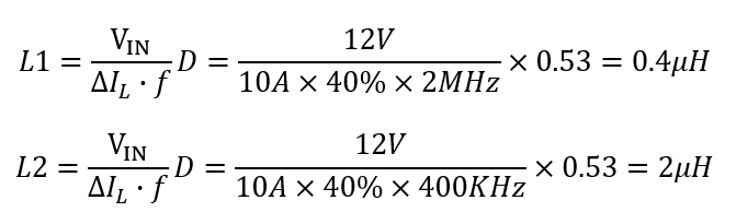
Calculate the inductor (L1) for 2MHz switching frequency and the inductor (L2) for 400KHz.
ΔIL is calculated as 40% of load current.
At 2MHz, the inductance value is about 1/5, so the number of inductor turns is reduced.
Selection of output capacitor
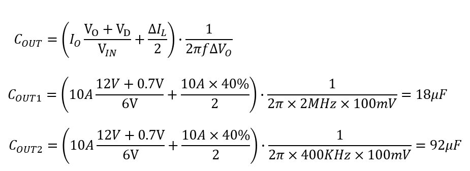
Calculate the value of the output capacitor. The output capacitor is determined by the allowable output ripple value. You can use the following formulas for calculations:
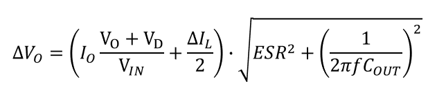
ESR in Equation 3 represents the ESR of the output capacitor.
This time, we will perform a circuit simulation of an ideal boost converter, so if we simply expand the equation assuming that the ESR is zero, it will be as shown in Equation 4, which is the equation for determining the capacitance of the output capacitor.
I calculated the output capacitor (Cout1) for switching frequency 2MHz and the output capacitor (Cout 2) for 400KHz.
As a result, Cout1=18μF, Cout2=92μF, and the higher the switching frequency, the smaller the capacitance of the capacitor.
Now, let's check by simulation whether the desired output voltage can be obtained with the calculated inductor and output capacitor.
Operation check with LTspice
Use LTspice to verify using the calculated inductor and output capacitor for the ideal boost converter circuit in Figure 1.
Confirm that 12V output is obtained at switching frequencies of 2MHz and 400KHz and that the ripple voltage is also the same.
If you have LTspice installed, please download and check the LTspice circuit file below.
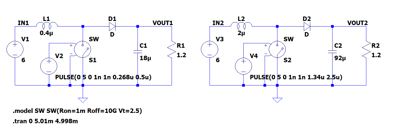
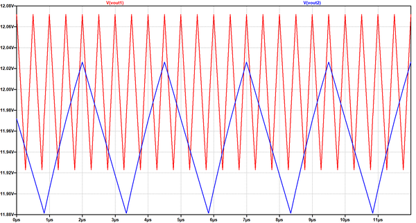
Figure 3 shows the output voltage simulation results.
Red (Vout1) is the result of switching frequency 2MHz, ripple is about 149mV at output voltage 12V
Blue (Vout2) is the result of switching frequency 400KHz, ripple is about 145mV at output voltage 11.95V
From these results, it can be said that there is no problem with the selected inductor and output capacitor, and in the case of a regulator with a high switching frequency, it was found that small parts such as inductors and capacitors used in the periphery can be selected.
However, there are some caveats.
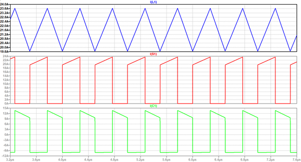
Check the various current waveforms in Figure 4. You can see that the blue inductor current has a low slew rate and is easily filtered by the input capacitor. However, you can see that the current flowing through the red switch and the current flowing through the green output capacitor are PWM current waveforms with a fast slew rate.
Careful attention must be paid to the design of the PCB layout where current with a high slew rate flows.
For the purpose of simulation this time, 2MHz and 400KHz are assumed to be similar slew rate simulation models. However, it can be inferred that the slew rate of 2MHz is faster than that of 400KHz in an actual device.
Summary
I hope you have understood that as the switching frequency increases, the size of the inductor and capacitor used in the regulator can be reduced.
However, higher switching frequencies present difficult challenges such as increased switching losses, high switch node slew rates, and high current slew rates. Also, finding a suitable MOSFET is difficult. The MOSFET should have low enough on-resistance to minimize conduction losses and be fast enough to allow fast switching. PCB component placement and routing should take PCB parasitic inductance into account and sensitive nodes should be free of noise propagation.
In the next article, I would like to use a simulation model of an actual regulator to confirm the effect of parasitic inductance in the PCB layout on current waveforms with a fast slew rate, and confirm points to note in PCB layout design.
Click here for recommended seminars/workshops
[Online Seminar] Analog Solution Power Supply Design Seminar <free>
[Online Seminar] Analog Solution Thermal Design Seminar <Free>
Click here for recommended articles/materials
Inquiry
If you have any questions regarding this article, please contact us below.
Analog Devices Manufacturer Information Top
To return to the Analog Devices manufacturer information top page, please click below.