- Semiconductor BusinessHOME
- Products and Services of Macnica,Inc.
-
technical information

-
Events and Seminars
- Handling Manufacturer
- Support
- Inquiry
- Click here to purchase products
- Semiconductor business e-mail magazine registration


 Narrow down by specifying conditions
現在2247件がヒットしています。check


FPGAs and CPLDs differ from ASSPs in that their uses and functions are fixed, and you can freely incorporate only the necessary functions.
It is an image of a designer creating (designing) a logic circuit in an empty box (although it is not actually empty), just like drawing a picture on a blank canvas. As much as we can design freely, RTL designers must organize and establish correct design methods for FPGAs and CPLDs and understand their characteristics. Instability such as "moved" can occur. These mostly come from timing issues. In other words, it is nothing other than “implementing a logic circuit with low reliability”.
In order to build highly reliable logic circuits, it is important to learn the basics of design techniques, which are key points in RTL design of FPGAs and CPLDs.
This time, before introducing the description technique, I would like to touch on the "differences between synchronous and asynchronous design" in digital logic circuit design.
A must-see for first-time FPGA/CPLD RTL designers.
FPGA/CPLD design is all about synchronous design!
This is not limited to Intel's FPGAs and CPLDs, but is common to all FPGA/CPLD manufacturers.
To understand it, let's first understand the advantages and disadvantages of synchronous and asynchronous.
What is a synchronous circuit
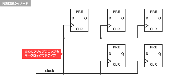
"A circuit system that operates in synchronization with the same edge of the same clock".
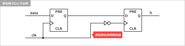
Therefore, even if they are the same clock, they are not regarded as the same clock if they use opposite phase edges.
Also, basically single clock synchronization is preferable. Sending and receiving signals between different clocks is an asynchronous circuit, and appropriate processing for asynchronous inputs is required.
| Advantages of synchronous circuits | Disadvantages of synchronous circuits |
|
|
A design example of synchronous design is shown in VHDL description and VerilogHDL description.
| VHDL | Verilog HDL |
| library ieee; use ieee.std_logic_1164.all; use ieee.std_logic_unsigned.all; entity s_counter is port ( clk : in std_logic; enable : in std_logic; q : out std_logic ); end s_counter; architecture sync_pld of s_counter is begin process (clk) variable cnt : std_logic_vector(2 downto 0); begin if enable = '0' then cnt := cnt; elsif (rising_edge(clk)) then cnt := cnt + 1; end if; q <= cnt(2); end process; end sync_pld; |
module s_counter (clk, enable, q);
|
What is an asynchronous circuit
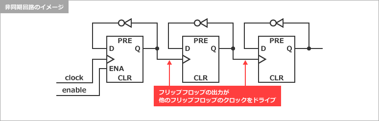
It means "a circuit system that does not operate in synchronization with the same edge of the same clock".
Therefore, even if the clock is the same, the circuit that operates with different clock edges is an asynchronous circuit.
Ripple clocks are a prime example. In addition, reusing the internally divided output also becomes an asynchronous clock with respect to the source clock.
| Advantages of asynchronous circuits | Disadvantages of asynchronous circuits |
|
|
Design examples of asynchronous design are shown in VHDL description and VerilogHDL description.
| VHDL | Verilog HDL |
|
library ieee;
end async_pld; |
module a_counter (clk, enable, q); cnt0 = ~cnt0; cnt0 = cnt0; |
Design examples using anti-phase clocks are shown in VHDL description and VerilogHDL description.
| VHDL | Verilog HDL |
| library ieee; use ieee.std_logic_1164.all; entity rev_clk is port ( clk : in std_logic; data : in std_logic; q : out std_logic ); end rev_clk; architecture rev_clk_pld of rev_clk is signal int0, int1: std_logic; begin process (clk) begin if (rising_edge(clk)) then int0 <= data; else int0 <= int0; end if; end process; process (clk) begin if (falling_edge(clk)) then int1 <= int0; else int1 <= int1; end if; end process; q <= int1; end rev_clk_pld; |
module rev_clk (clk, data, q); input clk, data; output q; reg int, q; always @(posedge clk) int = data; always @(negedge clk) q = int; end module |
Based on the above
Synchronous design with a single clock is the basic concept for ensuring high design quality in systems using FPGAs and CPLDs.
As FPGAs/CPLDs grow in scale, device vendors are proposing various interconnect schemes to ensure flexibility while maintaining high speed.
However, it is practically impossible to arrange the delays in all devices so that they are uniform throughout a single device.
Additionally, these delays often vary due to external factors such as voltage fluctuations, ambient temperature, and lot variations.
An asynchronous design under these conditions creates a race between clock and data signals. Occasionally, a "skipping" condition occurs where the data overtakes the clock.
To prevent this, it is necessary to perform synchronous design while maintaining the worst-case conditions recommended by Intel.
As long as you do a synchronous design, the clock skew is adjusted to the minimum inside the device, so you don't have to worry about ``dropping out''.
Therefore, the only thing to be careful about is securing the setup time and hold time of the input signal from the outside.
I would like you to be conscious of these points and build a more reliable digital logic circuit design.
This time, I explained about synchronous and asynchronous circuits, which are the basics of FPGA / CPLD design.
Click here for recommended articles/materials
What exactly is an FPGA?
[Must-See for RTL Design Beginners] The Impact of Asynchronous Signal Input on a System
Regarding the operating characteristics of FPGA/CPLD