- Semiconductor BusinessHOME
- Products and Services of Macnica,Inc.
-
technical information

-
Events and Seminars
- Handling Manufacturer
- Support
- Inquiry
- Click here to purchase products
- Semiconductor business e-mail magazine registration
![]()
![]() Narrow down by specifying conditions
Narrow down by specifying conditions
現在2164件がヒットしています。check

In circuit design, there are cases where the component mounting area on a board is limited due to demands for product miniaturization, and cases where consolidation of multiple components is required to reduce total BOM costs. By using GreenPAK from Renesas Electronics Corporation (hereinafter referred to as Renesas), such demands can be met. In this article, we will introduce how GreenPAK is being used, highlighting actual examples from circuit design sites.
What is GreenPAK?
Renesas' GreenPAK is an ultra-small digital-analog programmable IC. It consolidates the functions of multiple ICs and discrete components into a single chip, and can be customized to meet your needs. It is possible to implement functions similar to those of discrete components, including logic ICs, ADCs/DACs, clocks, comparators, and the associated components, in a GreenPAK.
To create your custom specifications, use the Go Configure™ Software Hub (a free tool).
Challenges of miniaturizing power supply systems
This time, I would like to introduce some examples that occurred in actual development sites and use them as a basis for implementation.
The power supply system under consideration was as shown in Figure 1.
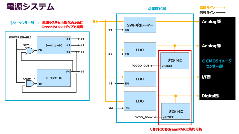
As shown in Figure 1, power supply systems are broadly divided into three configurations.
①CMOS image sensor section
② Power supply IC section (supplies power to the CMOS image sensor)
③Sequencer section (controls the ON/OFF of each power supply IC)
When considering a power supply system,
"There is not enough space on the board to mount ICs, so we want to simplify the power supply system configuration."
We faced the following challenge.
Therefore, we began investigating whether we could solve the above issues by implementing the sequencer section on a single GreenPAK chip.
Power supply sequencer implementation procedure using GreenPAK
Circuit to be implemented in GreenPAK
The required specifications and configuration of the sequencer part in this power supply system are as follows:
[Required specifications for the sequencer]
- Capable of controlling the ON/OFF of four power supply ICs (1 SW regulator, 3 LDOs)
・The order of the ON sequence of each power supply IC is #1→#2→#3→#4
・The order of the OFF sequence of each power supply IC is #4 → #3 → #2 → #1.
・ON/OFF sequences must be performed within 200 ms each
・Sequencer power supply is 5V
[Sequencer section configuration]
As shown in the previous system diagram, the system is configured as follows:
・Sequencer IC × 2
・OR gate logic × 1
・AND gate logic × 1
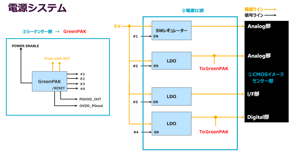
The [sequencer section configuration] will be replaced with 1 GreenPAK, and at the same time, the [required specifications for the sequencer section] will be realized.
In addition, the two reset ICs in the power supply IC section can also be consolidated into the GreenPAK.
Creating a power supply sequencer circuit with GreenPAK
First, open the GreenPAK circuit creation tool: Go Configure™ Software Hub.
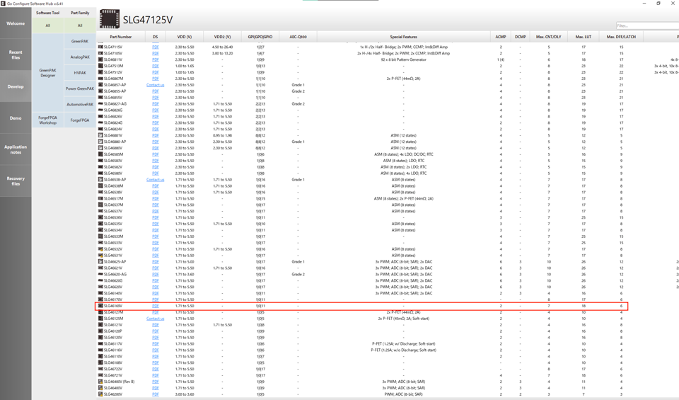
In the model number selection screen in Figure 3, select the GreenPAK model number that has the resources to realize the specifications this time. In this case, one 4-output power supply sequencer and two reset ICs will be mounted on the GreenPAK. Taking into consideration the number of required I/O, CNT/DLY, ACMP, etc., we decided on the SLG46169V.
CNT/DLY: Required for delay circuit
ACMP: Required for voltage detection of the reset IC
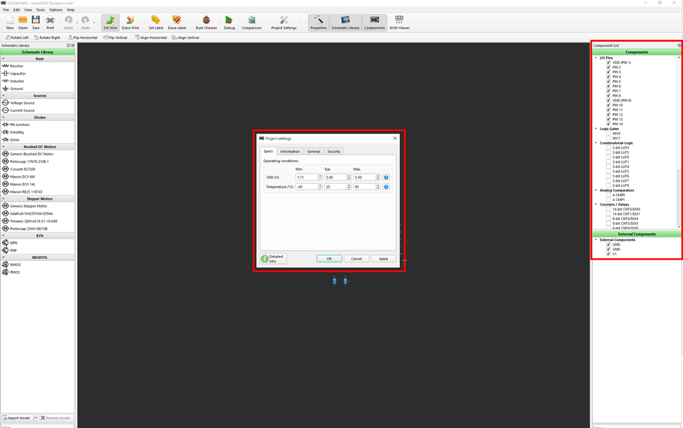
In Figure 4, double-clicking the model number will open the Go Configure development screen. In the middle window, specify the power supply voltage range for the device. In this example, specify Typ. 5.0V.
Next, we will actually create the circuit. Check the macrocells to be used in the "Components" window on the right side of the screen, and each macrocell will appear in the Work Area in the center of the screen.
[Cells used this time]
■ Power supply sequencer section
- 5 I/O pins
- 4 x 3-bit LUTs
・CNT/DLY x4
・OSC (built-in oscillator) x 1
■ Reset circuit section
- I/O pins x 4
- 2-bit LUTs x 2
・CNT/DLY x2
- ACMP (analog comparator) x 2
Once the macrocells are placed, create the power sequencer circuit. For instructions on creating the reset circuit, see I tried making a reset IC with GreenPAK To configure the power supply sequencer circuit, each macrocell is wired as shown in Figure 5.
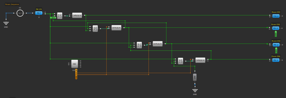
Double-clicking the CNT/DLY cell that creates the delay will display the Properties window on the left side of the screen. Leave the reference clock at its default setting and set the Counter data value to any value to determine the Delay time. In this example, the four power supply ICs must start up within 200 ms, so set the Counter data value so that the Delay time for each CNT/DLY cell is approximately 40 ms (set all CNT/DLY cells in the same way).
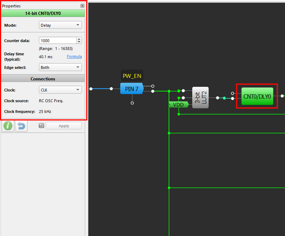
Next, to create the logic for the power-up and power-down sequences, double-click the 3-bit LUT cell. The truth table will be displayed in the Properties window on the left side of the screen, so set the output values as shown in Figure 7 (make the same settings for all 3-bit LUT cells).
At this point, the circuit creation and macrocell settings are complete.
〇 Simulation check
Using the simulation software on Go Configure, we will check whether the power sequencer circuit we created works as expected.
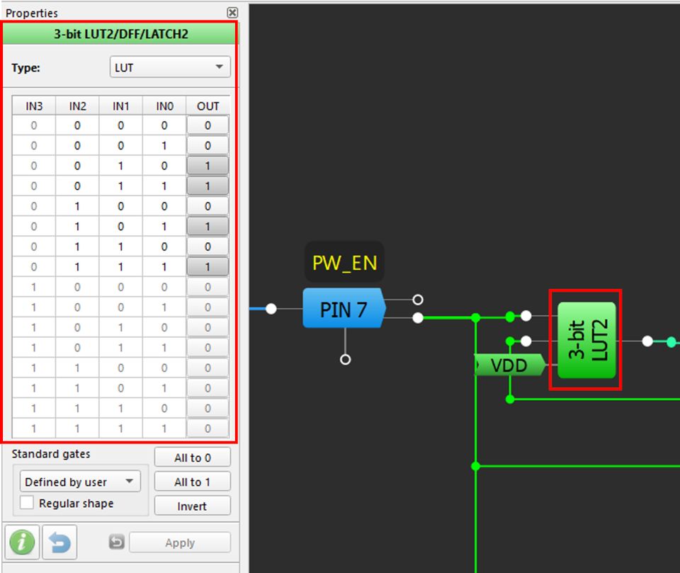
Select the "Schematic Library" tab at the bottom of the left window screen to switch windows, then click "Voltage Source" in the window and place it in the Work Area. Connect the + side to the input port and the - side to GND as shown in Figure 8.
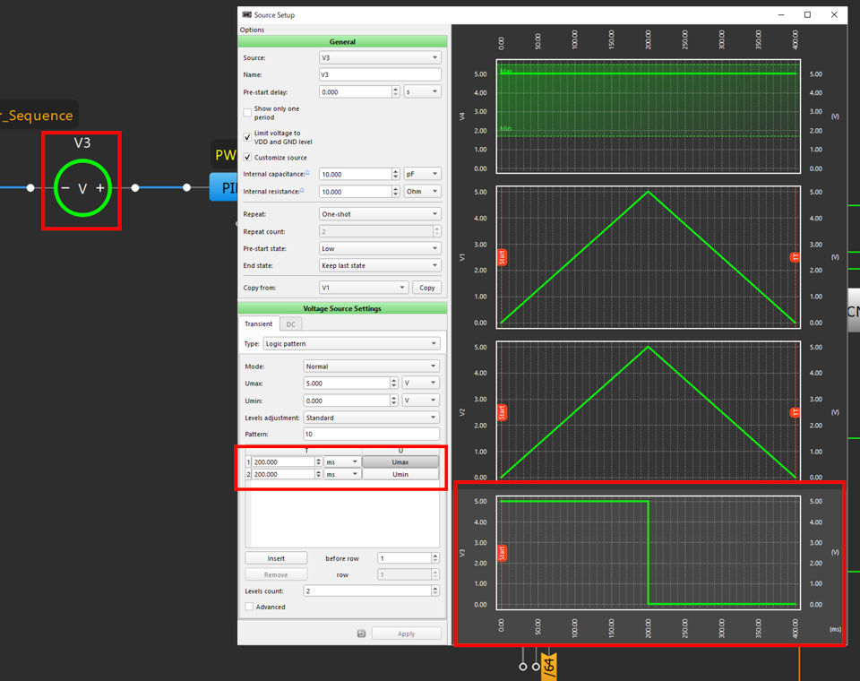
Double-click the Voltage Source symbol to display the signal setting screen. Here, you can set the waveform you want to input. In this case, the power supply sequencer receives the Enable signal as an input signal.
Set the input waveform to Hi: 200 ms, Lo: 200 ms, as shown in Figure 9, so that you can confirm that the specified ON sequence is performed after a Hi-level Enable signal is input, and that the specified OFF sequence is performed after a Lo-level Disable signal is input.
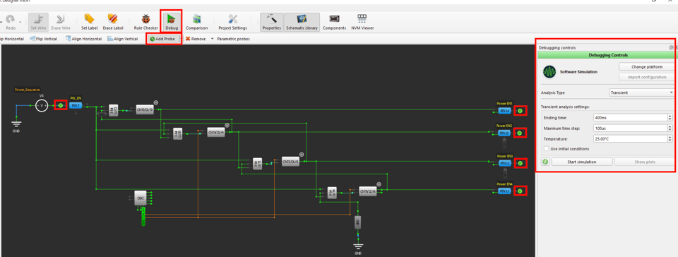
To start the simulation, click "Debug" at the top of the screen, and with "Add Probe" selected, place a probe symbol where you want to measure the waveform.
Next, in the right window, set the Ending time to 400ms and the Maximum time step to 100μs, and click “Start simulation”.
The simulation waveform is shown below.
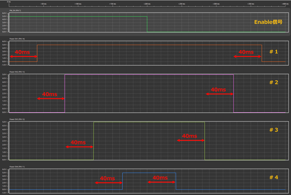
You can see that upon receiving a high-level Enable signal, each of the four signals rises with a delay of about 40 ms in the following order: #1 → #2 → #3 → #4.
When the Enable signal drops to the Low level, you can see that each of the four signals falls with a delay of about 40 ms in the order of #4 → #3 → #2 → #1.
Summary
We have introduced the steps to create a power supply sequencer circuit using GreenPAK, taking up an actual example from a development site. In this example, we consolidated multiple ICs onto a single chip, flexibly set the delay amount without using an external capacitor, and confirmed the validity of the circuit by simulating it on software. The GUI operation is also intuitive and easy to understand, so we hope you will make use of this product.
Contact us