- Semiconductor BusinessHOME
- Products and Services of Macnica,Inc.
-
technical information

-
Events and Seminars
- Handling Manufacturer
- Support
- Inquiry
- Click here to purchase products
- Semiconductor business e-mail magazine registration
![]()
![]() Narrow down by specifying conditions
Narrow down by specifying conditions
現在2189件がヒットしています。check
![[Series Article] The Fabulous Properties of Bipolar Transistors That Seem to Disappear but Won't Disappear ~ Series 2: Vceo and Vces](/business/semiconductor/articles/146947_Onsemi_articel_cover.png)
In the second installment of this series, we will explain Vceo (collector-emitter voltage) and Vces (collector-emitter breakdown voltage).
Collector-emitter voltage Vceo
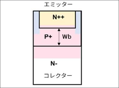
Vceo is the breakdown voltage when the depletion layer that spreads from the base to the emitter and the depletion layer that spreads from the EB junction to the base collide.
(See Figure 5 on the left below)
This is the same location for both discrete and planar structures; once the base width (Wb) directly below the EB junction in Figure 5 and Vcbo are determined, Vceo is determined by this base width (Wb).
Now, this base width (Wb) is actually one of the physical factors that determine hFE.
The wider the base width (Wb), the lower the hFE; the narrower the base width, the higher the hFE.
Furthermore, when making transistors using the conventional thermal diffusion method, it is difficult to control this point, and it is generally said that hFE varies from 1/2 to the target value to 2 times.
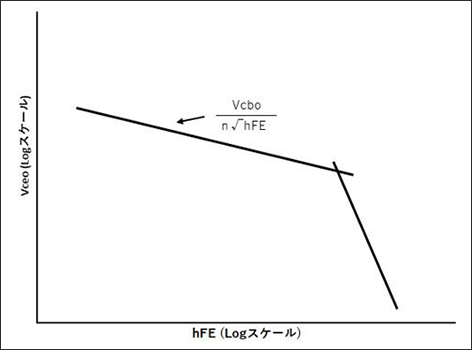
If we express what we have discussed so far in a formula,
The relationship is Vceo = Vcbo/n √h FE.
n is a coefficient determined by experiment.
If there are manufacturers currently developing new bipolar transistors, they may be calculating n using T-CAD (process simulation tool).
To find n through an experiment, vary hFE and create the graph shown in Figure 6 on the right below. The slope of the line is n.
Collector-emitter breakdown voltage Vces
Next, I would like to explain about Vces.
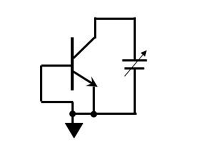
Vces is the withstand voltage between the collector and base when the emitter and base are shorted, as shown in Figure 7.
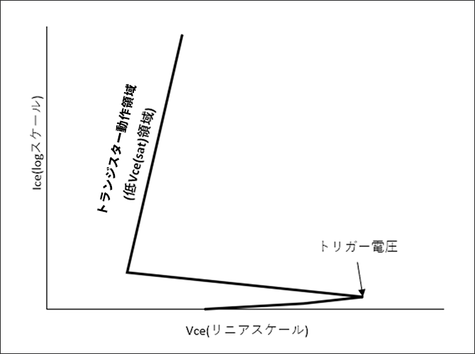
Since the EB is short, what happens to the withstand voltage waveform? In fact, the withstand voltage waveform is completely different between DC measurement and pulse measurement.
When DC measurements are made using a curve tracer, the waveform appears as shown in Figure 8 below.
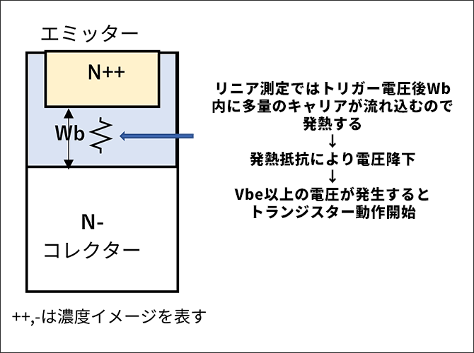
This is because minority carriers injected into the base and heat generation cause a voltage drop within the base width (Wb), resulting in transistor operation (see Figure 9 below right).
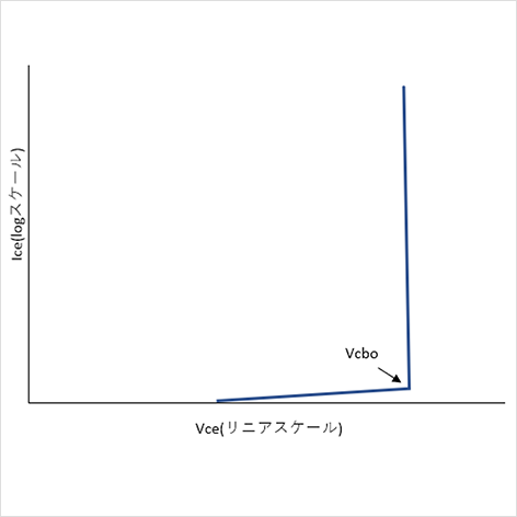
The withstand voltage waveform in pulse measurement is the same as Vcbo (see Figure 10 on the right).)
Young engineers who normally use an SMU (source measurer unit) on a power supply to measure transistor characteristics may not have yet experienced the difference in waveforms between DC and pulse measurements and may need advice from a veteran engineer.
Now, the reason why Vces for a pulse waveform is the same as Vcbo is that with a pulse input, heat generation in the base width (Wb) is low and no voltage drop occurs, so the diode characteristics are simply measured.
In other words, if you provide it with enough energy to generate heat within the base width (Wb), it will function as a transistor.
Generally, when EB is shorted, the emitter is grounded, and the collector is biased, it is called an off-transistor. In ICs, this form is often used as an element to prevent electrostatic destruction, which has high energy. By adjusting the base width (Wb), the operating voltage for electrostatic pulses can be set in any way, making it extremely useful as an electrostatic destruction protection element.
In the next installment of this series, we will explain the emitter-base junction voltage Vebo.
To the serial article list page
To see a list of articles in this Transistor series and other articles, please click below.
Inquiry
If you are interested in the content introduced in this article, please feel free to contact us.
Onsemi Manufacturer information Top
If you want to go back to ONSEMI Manufacturer Information Top, please click below.