- Semiconductor BusinessHOME
- Products and Services of Macnica,Inc.
-
technical information

-
Events and Seminars
- Handling Manufacturer
- Support
- Inquiry
- Click here to purchase products
- Semiconductor business e-mail magazine registration
![]()
![]() Narrow down by specifying conditions
Narrow down by specifying conditions
現在2158件がヒットしています。check
![[Serial Article] The wonderful characteristics of bipolar transistors that seem like they will disappear but won't disappear ~ Series 1: Collector-base breakdown voltage Vcbo](/business/semiconductor/articles/146838_Onsemi_articel_cover.png)
preface
Approximately 70 years have passed since the invention of the silicon bipolar transistor.
In the early 2000s, analog MOS wafer processes and circuit technology improved dramatically, and it was temporarily said that bipolar transistors might disappear, but they are still alive and well today. I would like to explain the characteristics of bipolar transistors (hereafter referred to as transistors) in a casual manner.
Transistor withstand voltages include Vcbo, Vceo, Vebo, and Vces, and characteristics include hFE, Vce(sat), SOA, ft, etc., and when initially selecting components, these data are often looked at.
In the first part of this series, I would like to talk about the collector-base voltage, Vcbo.
Collector-base breakdown voltage Vcbo
Usually, explanations of breakdown voltage are based on energy band gap diagrams, but I often find it difficult to visualize what is being said when explained using a band gap diagram.
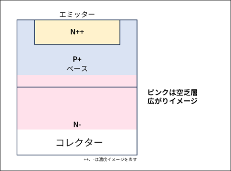
So we came up with the image shown in Figure 1, below on the left.
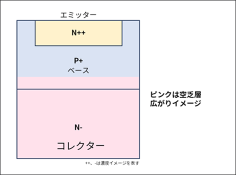
Figure 1 shows the spread of the depletion layer in silicon. In the case of a CB (collector-base) junction, the carrier concentration in the base is higher than in the collector, so the depletion layer spreads mainly to the collector. The more this depletion layer in the collector spreads, the higher Vcbo becomes. When this depletion layer reaches its limit, in other words, the collector electrode, it enters a breakdown state as shown in Figure 2 on the lower right.
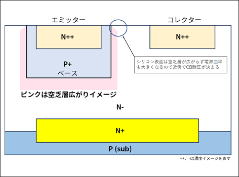
What we've discussed so far has actually been about discrete devices.
In the case of a planar IC structure, the breakdown voltage is determined at a different location. Figure 3 on the bottom left highlights the base diffusion layer in a planar IC.We need to explain how silicon crystals form in this way, so The Vcbo of a planar structure is determined by the lateral spread of the irregular depletion layer. If you have ever seen traces of overvoltage destruction on an IC, you will understand, "I see, that's where it broke."
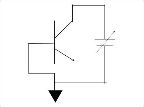
Vcbo The measurement circuit is shown in the lower right figure. 4 That's all for the explanation of Vcbo.
To the serial article list page
To see a list of articles in this Transistor series and other articles, please click below.
Inquiry
If you are interested in the content introduced in this article, please feel free to contact us.
Onsemi Manufacturer information Top
If you want to go back to ONSEMI Manufacturer Information Top, please click below.