- 半導体事業HOME
- マクニカの製品・サービス
-
技術情報

-
イベント・セミナー
- 取扱メーカー
- サポート
- お問い合わせ
- 製品購入はこちら
- 半導体事業のメルマガ登録
![]()
![]() 条件を指定して絞り込む
条件を指定して絞り込む
現在2003件がヒットしています。check

前回、CMOSイメージセンサーの動作を理解する上で基本となる光電変換について説明しました。
*前回の記事はこちら→CMOSイメージセンサーが光を取り込むための入り口、光電変化について
CMOSイメージセンサーは埋込まれている受光素子で内部光電効果の仕組みを利用して光を電荷に変えていること、そして、半導体の持つバンドギャップによって取込める光の波長が決まっていることを説明しました。例えば、シリコン (Si) のバンドギャップは1.1eVであり、波長1100nm以下の光を取込むことができます。
では、波長1100nm以下の波長の光であれば何でも電荷に変えることができるのか?と思うかもしれませんが、実際にはそうではなくSiの受光素子を持つCMOSイメージセンサーでは約300nm~1100nmの波長の光を取込み、300nmより短い光は取込むことが難しくなってきます。その理由は、物質には吸収係数が決まっているためです。今回は、吸収係数について説明します。
吸収係数とは半導体を含む全ての物質の中を光、電磁波、放射線、音波などが進むときに単位長辺りにどのくらい吸収されるのかを示した定数です。CMOSイメージセンサーの受光素子に使われているSiでは横軸を波長 (nm)、縦軸を吸収係数α (cm-1) で表すと次のような特性になります。
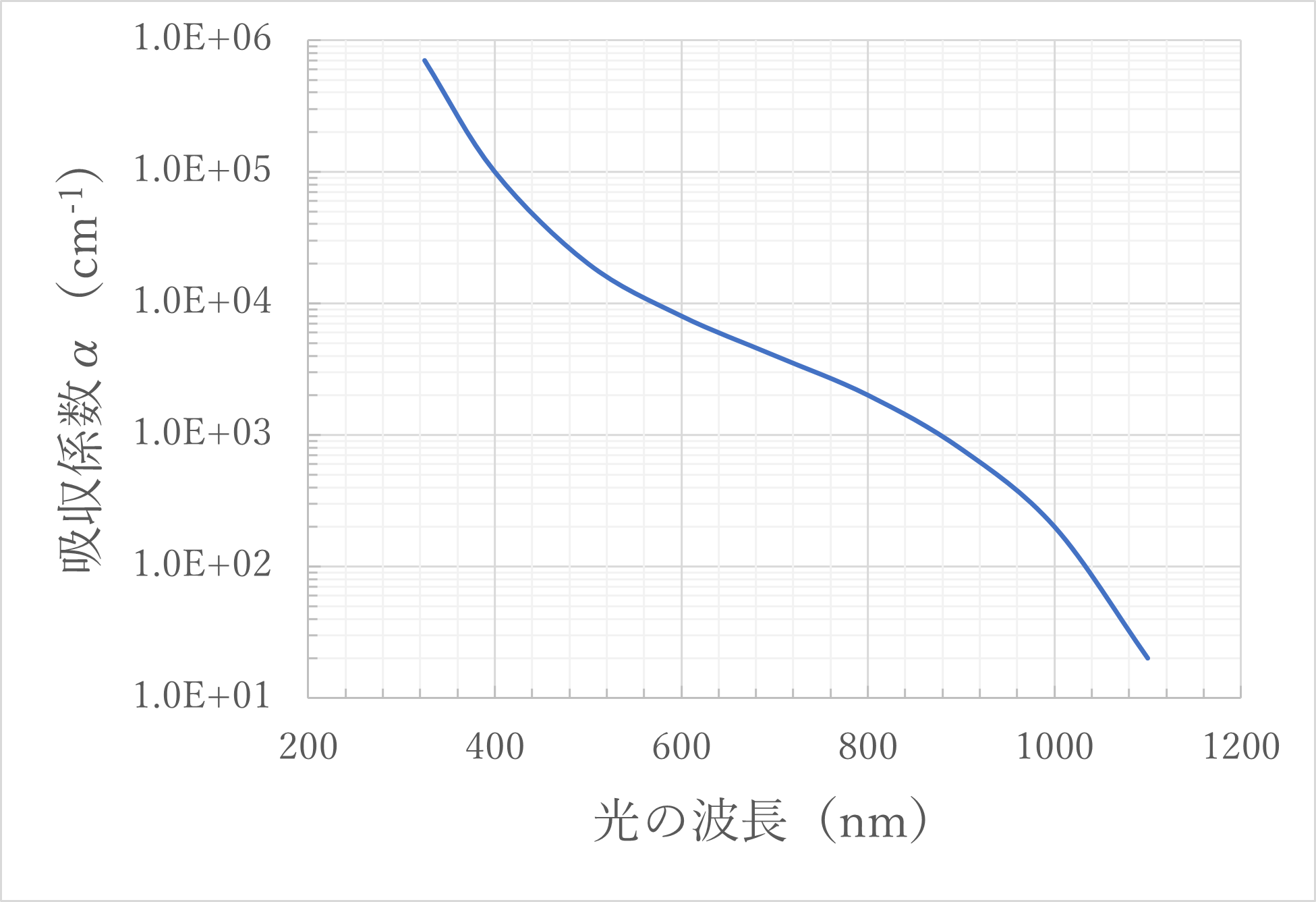
この吸収係数は物質によって決められており、例えばX線検査装置で使われるシンチレーターも基本的には同様の原理で動いています。
さて、半導体を含む物質に光が入射したときに、物質表面から深さx (cm) の位置における光強度Iは次の式で表すことができます。
ここでI0は物質表面x=0(cm)での光強度、αは吸収係数を表します。
この式に先ほどのSiの吸収係数を当てはめて、縦軸を波長毎の光強度 (%)、横軸を光が侵入する深さ (um) を表すと次のような特性になります。
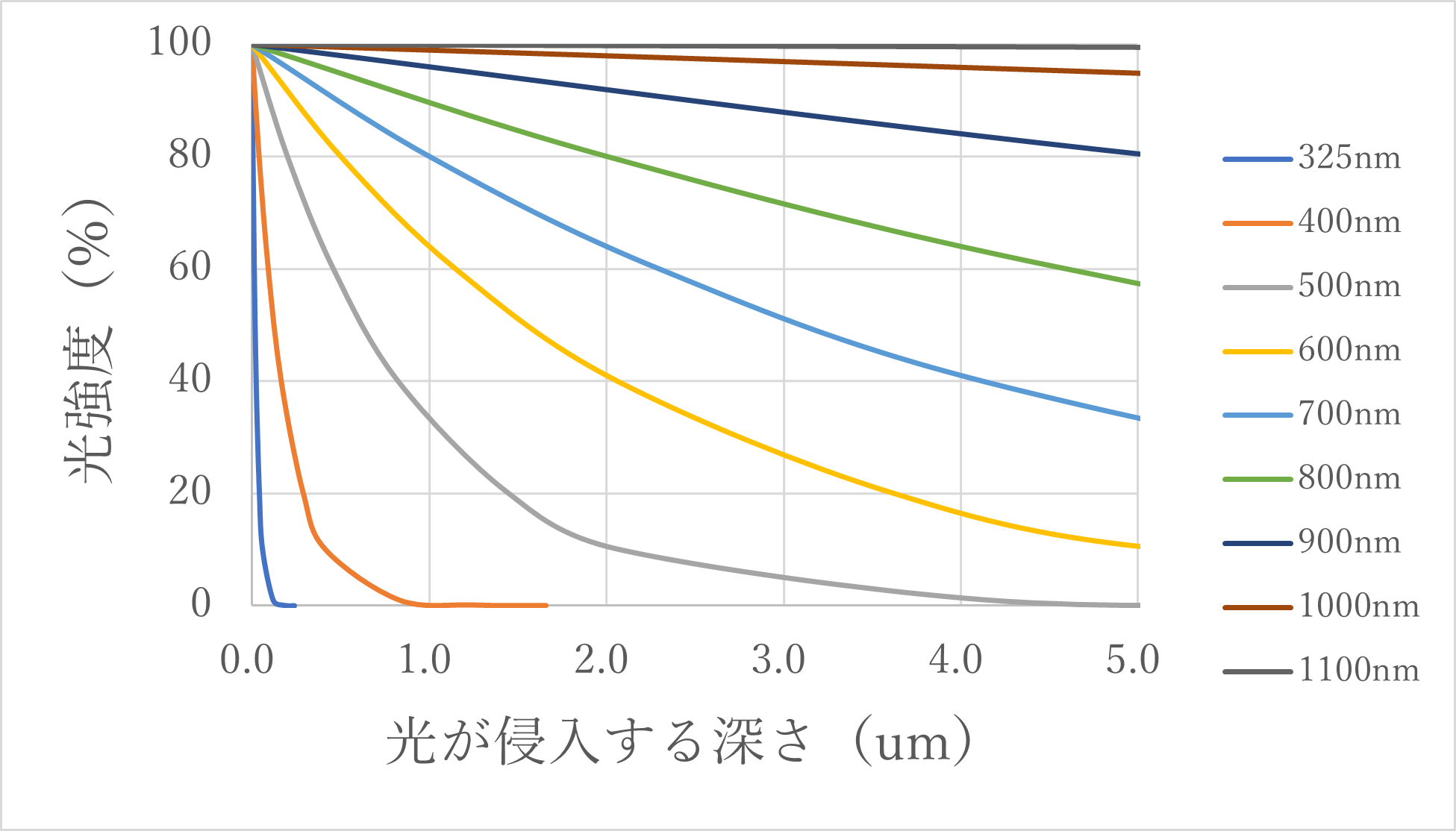
この特性から波長の短い光であればあるほど物質の表面までしか光が届かず、波長の長い光であればあるほど物質の中まで光が届くことが解ります。
受光素子がSiで作られたCMOSイメージセンサーで青い光を当てても上手く撮影できない理由は波長の短い青い光はSiの内部まで侵入せず、十分に光電変換がおこなわれないことが原因です。
このように前回説明した光電変換と吸収係数の特性を活かして、CMOSイメージセンサーの受光素子は設計されています。
さいごに
今回は、CMOSイメージセンサーを理解する上で大事な吸収係数について説明しました。
この記事がCMOSイメージセンサーの理解を深める一助となればと思います。
お問い合わせ
本記事にて紹介した製品に、ご興味がある方は、ぜひお問い合わせください。
オンセミ メーカー情報Topへ
オンセミ メーカー情報Topに戻りたい方は以下をクリックしてください。