- Semiconductor BusinessHOME
- Products and Services of Macnica,Inc.
-
technical information

-
Events and Seminars
- Handling Manufacturer
- Support
- Inquiry
- Click here to purchase products
- Semiconductor business e-mail magazine registration
![]()
![]() Narrow down by specifying conditions
Narrow down by specifying conditions
現在2153件がヒットしています。check
When designing an AC-DC flyback power supply, the choice of control IC greatly affects the subsequent man-hours.
By selecting an appropriate control IC, you can greatly reduce the man-hours required for power supply design and support future expandability.
This paper introduces control ICs for AC-DC flyback power supplies that incorporate high-voltage switching FETs.
Switching power supply control ICs with built-in FETs (hereafter referred to as Switchers) have the following three advantages over control ICs with external FETs.
・ Small mounting space
・ Low cost
・ Easy power supply design
On the other hand, since the FET is fixed, there are also disadvantages such as limited solutions when problems such as insufficient efficiency, large heat generation, or noise that does not fall within the standard are encountered during evaluation.
Selecting the optimum control IC will help minimize these disadvantages.
This paper introduces the following:
- What kind of power supply should Switcher be used with?
- How to choose output and FET size
- Monolithic type and 2-chip type
- Series lineup is important
- Switching frequency affects efficiency and noise
- Overcurrent protection limit for drain current is most important
- FET drain withstand voltage also affects efficiency
- Noise countermeasures are troublesome and difficult
- Difficult transformer design without slope compensation
1. What kind of power supply should Switcher be used with?
Switcher is ideal for miniaturizing power supplies.
In the case of DIP-8 and SO-8 packages, we think that switchers on the market today have a possible output range of about 30W to 40W. Therefore, if output power below this and small size and low cost are important, Switcher is the best choice.
On the other hand, if you need more output than that, we recommend choosing a Switcher with a larger package or a control IC with an external FET.
2. How to choose output and FET size
If you look at the Switcher datasheet, you'll find a table listing the maximum power output as shown below.
The output of the power supply is determined to some extent by the capabilities of the FET built into the Switcher and the thermal resistance of the package. In practice, it depends on the heat dissipation design of the power supply, so the data in this table is for reference only.
An open frame means a power supply with no case and good heat dissipation to the surroundings, and an adapter means a power supply that is covered with a case and has limited heat dissipation to the surroundings.
Therefore, the Adapter's output is smaller than the Open Frame's.
Also, an input voltage range of 85 to 265VAC will result in a smaller output than 230VAC.
First, you can select a product by considering the output power listed in this table as the maximum output.
| Part number | PKGs |
Switching Frequency |
Max. RDS(ON) [Ω] |
Output Power Table [W] | ||
| Adapter | open frame | |||||
| 85~265V AC | 85~265V AC | 230V AC | ||||
| NCP11184A065PG | PDIP-7 | 65 kHz | 2.25 | 18 | 25 | 37 |
| NCP11185A065PG | 1.3 | 22 | 30 | 45 | ||
| NCP11187A065PG | 0.65 | 30 | 40 | 60 | ||
| NCP11184A100PG | 100 kHz | 2.25 | 18 | 25 | 37 | |
| NCP11187A100PG | 0.65 | 30 | 40 | 60 | ||
3. Monolithic type and 2-chip type
Switcher can be broadly divided into two product groups.
・Monolithic type
・2 chip type
|
|
Monolithic type |
2 chip type |
|
chip configuration |
FET and control circuit on the same chip |
Separate chip for FET and control circuit |
|
FET structure |
Horizontal |
vertical |
|
Cost performance |
Advantageous at low output |
Higher power is better |
|
Avalanche capability |
× |
○ |
The monolithic type forms a high-voltage switching FET and control circuit on a single silicon chip.
The 2-chip type integrates a control circuit chip and a discrete high-voltage switching FET into a single package.
The monolithic type FET has a horizontal structure with the drain and source located on the front side of the chip.
Discrete FETs used in two-chip types are usually vertical structures with the drain on the back side and the source on the front side. The higher the breakdown voltage and the lower the on-resistance, the vertical structure is advantageous for lower cost and smaller size.
Therefore, given the same chip size, the monolithic type FET has a higher resistance than the discrete FET due to the above structural reasons, so the higher the output, the more advantageous the 2-chip type is. .
In the past, due to high assembly costs, monolithic type products were the mainstream, and there were many low-priced products in the lineup. However, due to rapid improvements in assembly technology in recent years, 2-chip types have become less expensive. I was.
Also, if the package is limited, there is a limit to the chip size that can be mounted in the package, so a two-chip type that can mount a MOSFET with a lower resistance can achieve higher output.
Furthermore, one of the advantages of the 2-chip type is robustness.
In the case of monolithic devices, the high-voltage switching FET and the control circuit are formed on the same chip, so when a lightning surge or the like is applied to the FET terminal, latch-up occurs between the FET and the control circuit. and destroy it.
In the case of the 2-chip type, the FET and control circuit are physically separated, so this kind of latch-up does not occur and is highly resistant to lightning surges.
In addition, monolithic FETs generally have low avalanche tolerance and are not listed on spec sheets, whereas dual-chip FETs have avalanche tolerance listed on their spec sheets.
In this way, 2-chip type power supply control ICs have the advantages of high output, high efficiency, and robustness.
On the other hand, for low-power switching power supplies of a few watts, the size of the required FET is small, so a monolithic type Switcher may be more cost-effective.
4. Series lineup is important
When choosing a Switcher, it is important to check that the FET size, drain current limit, and frequency lineup are aligned.
When evaluating the power supply, problems such as a little lack of efficiency and a little heat generation frequently occur.
It would be nice if the transformer could be changed, but if that effect cannot be obtained or if the transformer cannot be changed, a product with a higher FET or a product with a different frequency or drain current limit must be selected from the same series. Otherwise, the PCB design would have to be redesigned or a major circuit overhaul would be required.
Therefore, it is necessary to select a product with a full lineup of series such as FET sizes.
5. Switching frequency affects efficiency and noise
Many switchers use a fixed frequency, current mode PWM control scheme.
(Recently, control methods that improve efficiency by reducing the frequency at light loads, such as Frequency Foldback, have become common, but in this article, we will refer to these as fixed-frequency current-mode PWM control methods. increase.)
Although there are some differences in the fundamental frequency depending on the manufacturer, three types of 60kHz, 100kHz, and 130kHz are commonly seen.
Frequency is closely related to efficiency and noise. Prioritizing efficiency and noise favors lower frequencies.
On the other hand, higher frequencies have the advantage that smaller transformer cores can be selected.
The frequency must be selected first, as transformer design will vary with this frequency.
6. Drain current overcurrent protection limit is most important
Along with the switching frequency, another important parameter in power supply design is the drain current overcurrent protection limit (ILIMIT).
In many Switchers, this ILIMIT is internally fixed and cannot be finely adjusted.
As I mentioned at the beginning, if the evaluation results show that the switcher is a little lacking in power, it will be replaced with a higher-grade IC, which will increase the cost of the system.
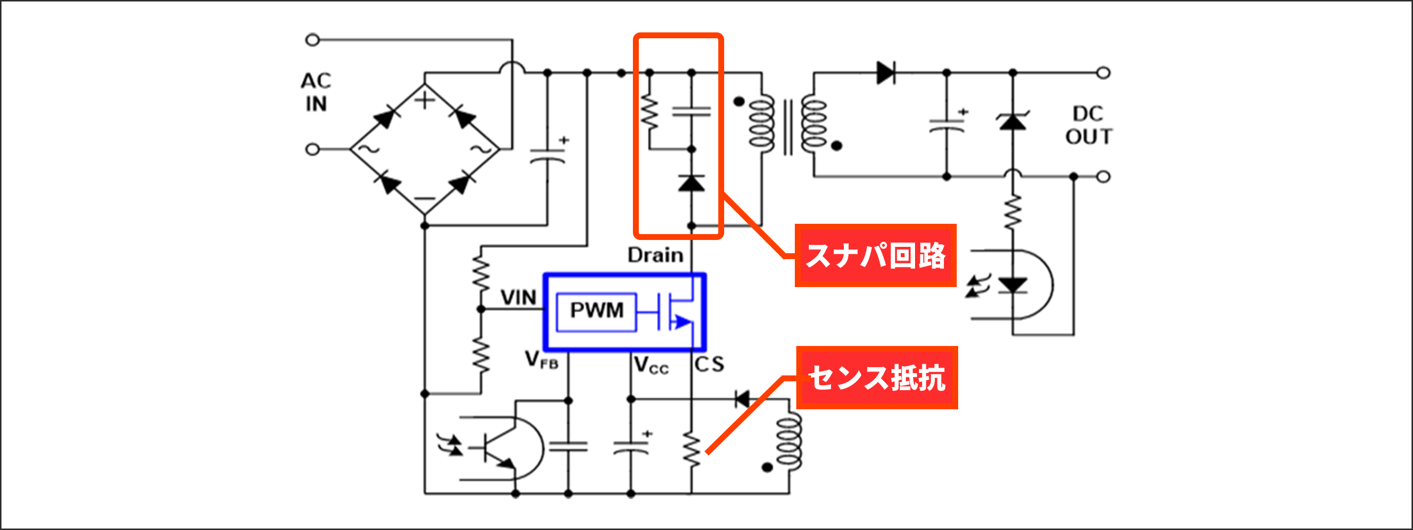
If the sense resistor that sets the ILIMIT is external and the product can be adjusted externally by the power supply designer, ILIMIT can be adjusted within the range that the FET allows, thus solving this problem easily. I can do it.
Additionally, ILIMIT also affects the drain voltage.
If ILIMIT is too large, the transformer core may saturate and the drain voltage may not have enough margin for the withstand voltage.
Again, being able to adjust ILIMIT externally is very useful for the power supply designer.
The advantage of this external sense resistor is that the drain current limit can be freely selected, which is the degree of freedom in design, and that a discrete resistor element is used, so that the drain current limit is highly accurate.
Since the sense resistor built into the control IC is made of a semiconductor element, it has greater temperature characteristics and variations than a discrete resistor element.
7. FET drain withstand voltage affects efficiency
Primary-side switching FETs used in AC-DC flyback power supplies normally require a withstand voltage of 600V or higher.
In particular, the drain voltage becomes the largest during startup, load fluctuation, and control mode switching.
When designing a power supply, it must be designed so that the drain voltage of the FET has a sufficient margin with respect to the absolute maximum ratings under all conditions.
Normally, as a countermeasure, a snubber circuit is used to absorb surge noise caused by leakage inductance.
Reducing the resistance value of the snubber circuit reduces the surge noise, but increases the loss in the snubber circuit and reduces the efficiency of the power supply.
Therefore, a high FET drain withstand voltage not only ensures safety, but also makes it possible to reduce the weight of the snubber circuit, which leads to improved efficiency.
8. Noise countermeasures are troublesome and difficult
A noise terminal noise test is conducted after a series of power supply evaluations has been carried out and the basic operation of the power supply has been confirmed. , countermeasures require experience and time.
If you add a noise countermeasure filter, you will have to redo the evaluation of efficiency and temperature again.
あらかじめノイズ対策の機能を持った製品を選ぶことで、電源設計の最後の工数を削減できます。
Quasi-resonant control (QR) and frequency jitter functions are common noise countermeasures for flyback power supplies.
There is another technology called Active Clamp, but it is expensive due to the increased number of parts, and there are no Switcher products that support Active Clamp, so I won't discuss it in this article.
Quasi-resonant control is an effective control method for noise and efficiency, but it always operates in discontinuous mode (DCM), and the heavier the load, the lower the frequency, so a large current must flow on the primary side. .
Compared to fixed frequency PWM control schemes, which can also operate in continuous mode (CCM), lower resistance FETs are required and the transformer core size is larger.
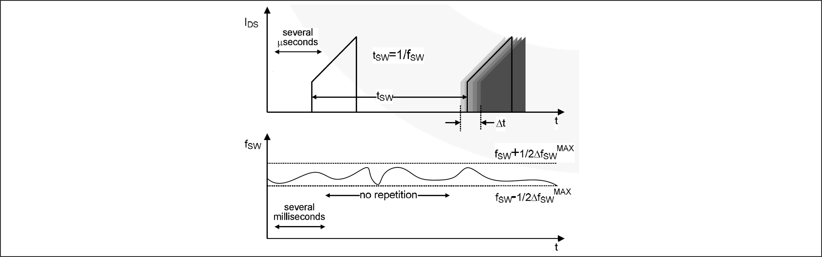
There are various methods and names for frequency jitter, such as frequency hopping and frequency modulation.
Although it is a simple technique, it has the effect of reducing EMI average noise, and can reduce noise countermeasure processes.
In addition, although this technology is not as effective as pseudo-resonance, it does not have any major disadvantages.
9. Difficult transformer design without slope compensation
Slope compensation is an effective feature to prevent subharmonic oscillations.
Some low-cost control ICs do not have this slope compensation.
If there is no slope compensation, the transformer must be designed so that the duty is 50% or less even in continuous mode (CCM) operation.
CCM operation and large duty are the conditions of low input voltage and heavy load.
If there is no slope compensation, CCM operation and duty is 50% or more, the operation becomes unstable due to subharmonic oscillation, noise occurs, and the overload protection operates at a load lower than the set value. There is fear.
Slope compensation allows more design latitude in power supplies.
ONSEMI has a large lineup of this Switcher together with power supply control ICs with external FETs, and is vigorously developing new technologies.
On the ONSEMI website, the FET external type is described as an offline controller, and the FET built-in type is described as an offline regulator.
If you are interested in our power control ICs and Switchers, please contact us using the inquiry button below.
Inquiry
On-semi maker information Top
If you want to go back to ONSEMI Manufacturer Information Top, please click below.