- Semiconductor BusinessHOME
- Products and Services of Macnica,Inc.
-
technical information

-
Events and Seminars
- Handling Manufacturer
- Support
- Inquiry
- Click here to purchase products
- Semiconductor business e-mail magazine registration
![]()
![]() Narrow down by specifying conditions
Narrow down by specifying conditions
現在2159件がヒットしています。check
We have a wide range of products that are perfect for powering circuits that need to be protected from noise, such as FPGAs, processors, and image sensors!
"NR1644" is a low-noise regulator that achieves both low noise and high PSRR.
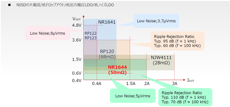
We also have a wide range of other low noise regulator products in our lineup: "NR1640", "RP122/123", "NR1641", and "RP120".
As electronic devices become more powerful and sophisticated, the power supply voltages that supply devices such as FPGAs, processors, and image sensors are becoming lower and larger in current, leaving engineers with a lot of headaches when it comes to selecting the right power supply.
As the voltage of the entire system becomes lower, the operating voltage margin is shrinking and the requirement for power supply accuracy is becoming stricter. In particular, when noise is superimposed on the power supply of a sensing device, the signal-to-noise ratio deteriorates. As the noise sensitivity of the power supply is increasing, power supply ICs are required to have high noise removal performance.
Nisshinbo Micro Devices is expanding its product lineup to address these challenges.
Overview of NR1644
The NR1644 is a product designed to address the market trends of higher current, lower voltage, and lower noise.
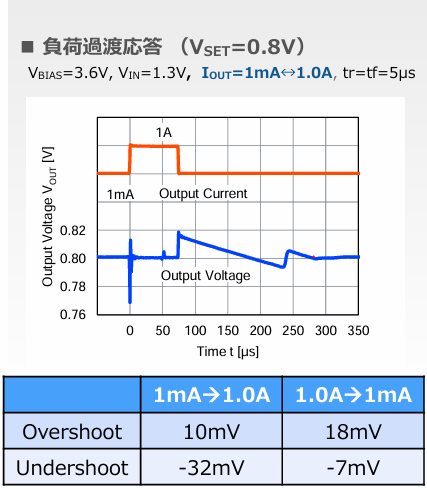
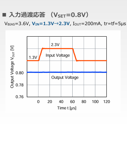
The required elements of low noise, high ripple rejection (high RR), low current consumption, high output current, and high-speed response are achieved at the highest level.
CMOS Image Sensor Power Supply
Let's take a look at the requirements for the CMOS Image Sensor (hereafter referred to as CIS) that this product targets and its functions for meeting those requirements.
In order to achieve high image quality with low power consumption, there is a strong trend toward lower operating voltages for CIS, and the voltage regulator that drives the CIS requires low-voltage output and
A stable power supply (higher current to improve image quality) and low noise are also essential.
The long-awaited NR1644 has been released as an LDO voltage regulator to solve these issues.
<Four features of NR1644>
・Large current 2.0A
・Low voltage output: 0.4V to 1.5V
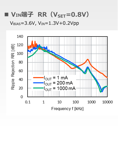
・Low noise Output voltage noise: 5uVrms (10Hz to 100kHz), Ripple rejection rate: 110dB@1k
-High output accuracy: ±1.0% (Typ)
| Civilian | |
|---|---|
| Input voltage range | V IN =VSET+VDO to VBIAS (Maximum rating: 6.5V) V BIAS =2.4V to 5.5V (Maximum rating: 6.5V) |
| Operating temperature range | TJ=-40°C to 125°C |
| current consumption | Typ.75µA |
| Standby Current | Typ.0.01µA |
| Output voltage range | 0.4V to 1.5V (0.1V step) |
| Output Voltage Accuracy | ±1.0% (Ta=25°C) |
| Input/Output Voltage Difference | Typ.90mV (IOUT=1 A) Typ.180mV (IOUT=2 A) |
| output current | 2000mA |
| Ripple Rejection Rate | Typ.110dB (f=1kHz, IOUT=1A) Typ.50dB (f=1MHz, IOUT=1A) |
| package | DFN2020-8-GA |
Switching regulator post filter
Another challenge is to eliminate ripple in the switching power supply, as the voltage accuracy requirements become stricter as the SoC core power supply voltage becomes lower.
The NR1644 is capable of low voltage output, supports output currents up to 2.0A, and achieves a well-balanced combination of high RR and high-speed response characteristics, making it effective as a post-filter for switching regulators.
It is equipped with a "PG (Power Good) terminal" as a function.
|
Terminal number
|
Terminal Name | I/O | function |
|
1
|
VIN
|
Power |
Power input terminal |
| 2 |
EN
|
I | Enable Terminal A "High" input sets the active state, and a "Low" input sets the shutdown state. It is pulled down by a constant current inside the IC. |
|
3
|
VBIAS | Power | Bias power supply input terminal Connect a capacitor between the VBIAS pin and GND. |
|
4
|
PG | O |
Power Good Terminal
NMOS open drain output. When the output voltage is equal to or higher than the PG pin "H" threshold voltage (VPGH), it outputs "High" (pull-up voltage). |
|
5
|
NR | - | Noise reduction capacitor connection terminal Please connect a capacitor between the NR terminal and GND. This capacitor reduces output noise and allows for adjustment of the soft-start time. |
|
6
|
GND | - | Ground terminal |
|
7
|
FB | I | Feedback Input Terminal Connect to the VOUT pin. |
|
8
|
VOUT | O | Output voltage terminal Please connect a capacitor between the VOUT pin and GND. |
Block Diagram
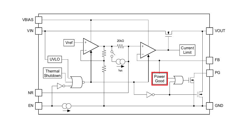
NR1644 Block Diagram
For detailed function information, please refer to the NR1644 datasheet.
Product lineup
Low noise regulators (consumer products) ideal for FPGAs, processors, and image sensors
*The in-vehicle compatible product is "NR1640 (200mA)"
*There are other automotive compatible 1A LDOs available in addition to those in the comparison table.
|
|
NR1644
|
RP120
|
NR1641
|
RP122
RP123 |
NR1640
|
|
Iout
|
2A
|
1.5A
|
1A
|
400mA
250mA |
200mA
|
|
Vin
|
2.4V-5.5V(6.5V)
|
2.4V-5.5V(6.5V)
|
1.7V-5.5V(6.5V)
|
1.9V-5.5V(6V)
|
2.7V-5.5V(6.5V)
|
|
Vset+Vdo~Vbias
|
Vset+Vdiff~Vbias
|
||||
|
Vset
|
0.4V-1.5V
|
0.6V-3.6V
|
1.0V-4.8V
|
1.2V-4.8V
|
2.5V-4.8V
|
|
Output Voltage Accuracy
|
±1%
|
±1.5%
|
±1%
|
±0.8%
|
±1%
|
|
Vdiff
|
0.18V
|
0.102V
|
0.15V
|
0.225V
|
0.13V
|
|
(Iout=2A)
|
(Iout=1.5A)
|
(Iout=500mA)
|
(Iout=400mA)
|
(Iout=200mA)
|
|
|
PSRRMore
|
110dB@1kHz
|
90dB@1kHz
|
90dB@1kHz
|
90dB@1kHz
|
80dB@1kHz
|
|
Output Noise
|
5uVrms
|
35uVrms
|
5uVrms
|
8uVrms
|
6uVrms
|
|
current consumption
|
75uA
|
35uA
|
17uA
|
9.5uA
|
350uA
|
|
Standby Current
|
-
|
0uA
|
0.01uA
|
0.01uA
|
0.1uA
|
|
package
|
DFN(PLP)2020-8-GA
|
WLCSP-6-P11
|
WLCSP1616-6-GY
|
PLP1010-4
|
SOT-23-5-DC
|
|
HSON-6-GU
|
WLCSP-4-P8
|
||||
|
Protection Circuit
|
TSD
Current Limit ISC Inrush(SS) |
TSD
Current Limit ISC Inrush |
TSD
Current Limit ISC |
TSD
Current Limit ISC Inrush |
TSD
Current Limit ISC |
|
function
|
Constant Slope
Auto Discharge Power Good High speed/low power consumption selection |
Constant Slope
Auto Discharge |
Constant Slope
ECO mode Auto Discharge |
ECO mode
Auto Discharge |
Constant Slope
Auto Discharge |
Purchase from Macnica-Mouser here
Inquiry
If you have any questions about this product or are interested in the evaluation kit, please contact us here.
Manufacturer information top
If you would like to return to the Nisshinbo Micro Devices manufacturer information top page, please click below.