- 半導体事業HOME
- マクニカの製品・サービス
-
技術情報

-
イベント・セミナー
- 取扱メーカー
- サポート
- お問い合わせ
- 製品購入はこちら
- 半導体事業のメルマガ登録
![]()
![]() 条件を指定して絞り込む
条件を指定して絞り込む
現在2168件がヒットしています。check

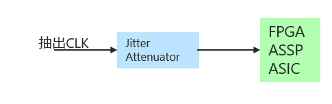
ジッタアッテネータについて
高速シリアルインターフェースのプロトコルが増え、高速ADC(Analog Digital Converter)、DAC(Digital Analog Converter)、信号処理用の高速FPGA等を使用するケースが増えています。Physical Layerで使用する高速インターフェース、ASSPなどを含め、Reference Clockのジッター/ワンダーに関する入力規定は、高速になればなる程、厳しくなっていきます。信号内に組み込まれたクロックを再生して使用するため、スクランブルや8B10Bの様な 0 または 1 がある程度連続しない様にして、データにクロックを埋め込み、クロックデータリカバリー回路(CDR)によって、受信したデータからクロックを再生します。
このクロックは、インターポレータ方式でリカバリーされることが多く、再生されたクロックには、伝送路の低域ジッター、ワンダーが含まれています。このジッターを含んだクロックをリファレンスクロックにして、FPGA内、ASSP内PLLで送信クロックを生成するとリファレンスクロックに含まれるジッターは、内部PLLの規定を満たさず、PLLの同期ができなかったり、ジッター、ワンダーが通過して、送信データのアイパターンの劣化に繋がります。このアイパターンの劣化により、送信データの規定を遵守することができない、受信側でのエラーレートの劣化などに繋がることが考えられます。
オーディオ製品では、全てのジッター、ワンダーがノイズとしてスピーカー、ヘッドフォンから漏れ聞こえることになります。そこで、ジッターを抑圧するために、ジッターアッテネーター、ジッタークリーナーの様なICを使用することが、推奨されます。
メーカーによってジッターアッテネーター、ジッタークリーナーやクロックコンディショナなど、呼称は変わりますが、IC内部の構成は同一のものです。
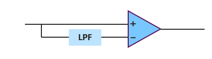
ジッターアッテネーター、ジッタークリーナーが出始めたころは、LPFによる構成が普通でした。そのため、LPFのカットオフ周波数を設定するレジスタを設定し、低域のジッターを低減する構成が採られていました。
その後、PLL ICの進歩によって、PLLが採用されるようになり、ジッターアッテネーター、ジッタークリーナーは共に内部の構成はDPLL+アナログPLLで構成される様になりました。中には、アナログPLLだけで構成される場合もあります。
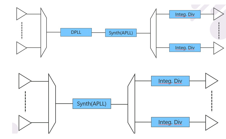
DPLLでジッターを除去し、アナログPLLで必要な周波数を生成します。DPLL、アナログPLLで使用されるVCOは両方とも内蔵の物とアナログPLLのみ外付けPLLが要求されるものがあります。DPLLは、ループ帯域を低くできるものもあり、リファレンスクロックに含まれるワンダーも除去できるものがあります。ワンダーの除去をおこなうには、DPLLのループ帯域を1Hz未満(ワンダーの周波数は、10Hz未満を指す)に設定するのが通常で、ループ帯域を低く設定すると、DPLLのロック時間が長くなるという弊害があります。
通常のラインカードで使用される帯域は、10Hz~20Hz程度が選択されます。このループ帯域を設定すると12Khzから20MHzのジッターは、除去することができ、送信規定を満たすことができます。次にアナログPLLですが、外付けのVCOを使用する場合、ジッターの安定度が良いVCOが必要です。VCOのジッターは、そのまま出力のジッターになるからです。アナログPLLで所望の周波数を作成し、出力をします。複数の周波数が必要な場合、フラクショナル分周回路を使用します。フラクショナル分周を使用すると出力に重畳するジッターが増えますので、送信に使用するクロックにはフラクショナル分周を使用しないのが普通です。
お問い合わせ
本記事に関してご質問などありましたら、以下よりお問い合わせください。
Microchip メーカー情報Topへ
Microchipメーカー情報Topページへ戻りたい方は、以下をクリックください。