- Semiconductor BusinessHOME
- Products and Services of Macnica,Inc.
-
technical information

-
Events and Seminars
- Handling Manufacturer
- Support
- Inquiry
- Click here to purchase products
- Semiconductor business e-mail magazine registration
![]()
![]() Narrow down by specifying conditions
Narrow down by specifying conditions
現在2164件がヒットしています。check

How to use Memory Base Register and Memory Limit Register
The PCIe interface is a widely used technology today, but it is a bit difficult to understand from the PCIe Specification alone, so this column will explain topics extracted from the specification.
This time, I will explain how to use the Memory Base Register and Memory Limit Register in the Type1 Configuration Space Header. Memory Base Register/Memory Limit Register is used to set Memory Rage, which is used by Bridge Devices such as PCIe Switches to determine whether or not to pass received Memory Transactions.
If the Memory Transaction is within the Memory Range set in Register, that Memory Transaction will be passed, but if it is outside the Memory Range, that Memory Transaction will not be passed.
Role of Memory Base/Limit Register
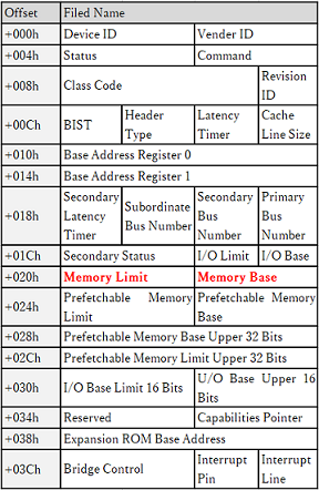
The roles of the Memory Base/Limit Register are as follows.
・Memory Base Register and Memory Limit Register consist of 16bits, and Memory Range consists of 32bits.
・The Memory Base Register sets the start address of the Memory Range, and the Memory Limit Register sets the end address of the Memory Range.
・The upper 12 bits of the Memory Base Register are the upper 12 bits of the Memory Range start address, and the upper 12 bits of the Memory Limit Register are the upper 12 bits of the Memory Range end address.
・The lower 20 bits of the memory range start address are fixed at 0x00, and the lower 20 bits of the end address are fixed at 0xFF.
Specific example of setting method
We will use a specific example to explain what values should be set. Please check the PCIe Specification for detailed specifications.
If you want to set the Memory Range through Memory Transaction to the range of E400_0000h - E40F_FFFFh, set the Register as follows.
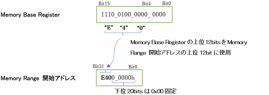
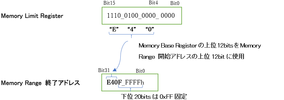
Memory Rage of E400_0000 - E40F_FFFF can be set by the register setting above.
Inquiry
If you have any questions regarding this article, please contact us below.