- Semiconductor BusinessHOME
- Products and Services of Macnica,Inc.
-
technical information

-
Events and Seminars
- Handling Manufacturer
- Support
- Inquiry
- Click here to purchase products
- Semiconductor business e-mail magazine registration
![]()
![]() Narrow down by specifying conditions
Narrow down by specifying conditions
現在2171件がヒットしています。check
Introduction
In the previous article, we introduced various cases for the MIPI interface, including how to use it in conjunction with an ASSP.
In this article, we will take a deeper look at FPGA MIPI interfaces while introducing the actual board configuration.
We hope that this information will be useful for your board design and device selection.
[Previous article] FPGA MIPI interface examples: 11 cases taking advantage of flexibility and high-speed processing
MIPI Interface Example: Holoscan Sensor Bridge Board
Why MIPI interface conversion is needed?
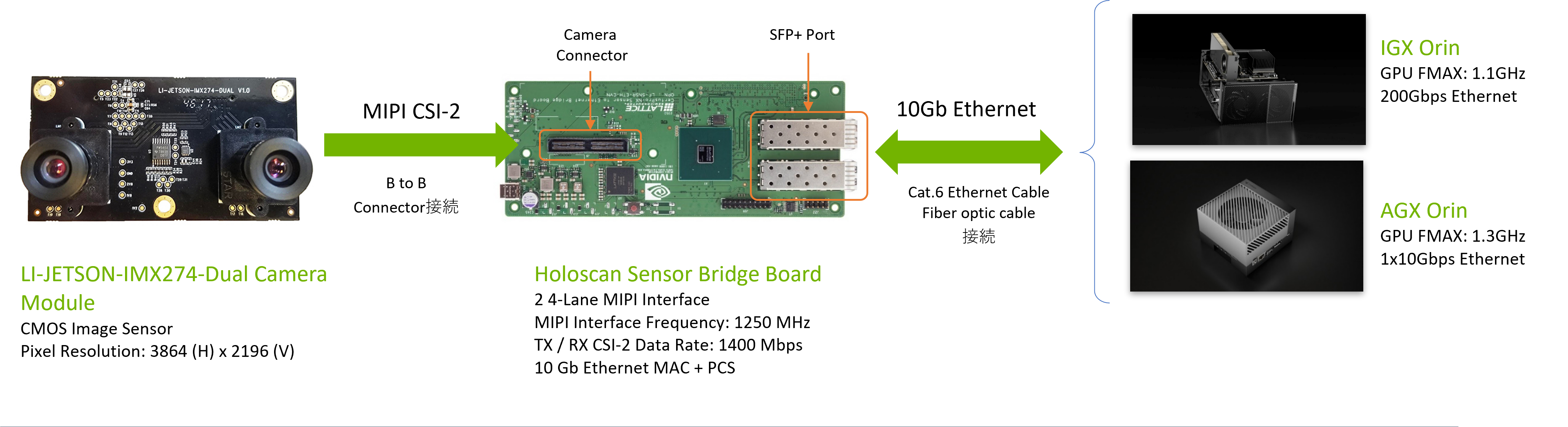
The example we will introduce this time is Lattice's Holoscan Sensor Bridge Board.
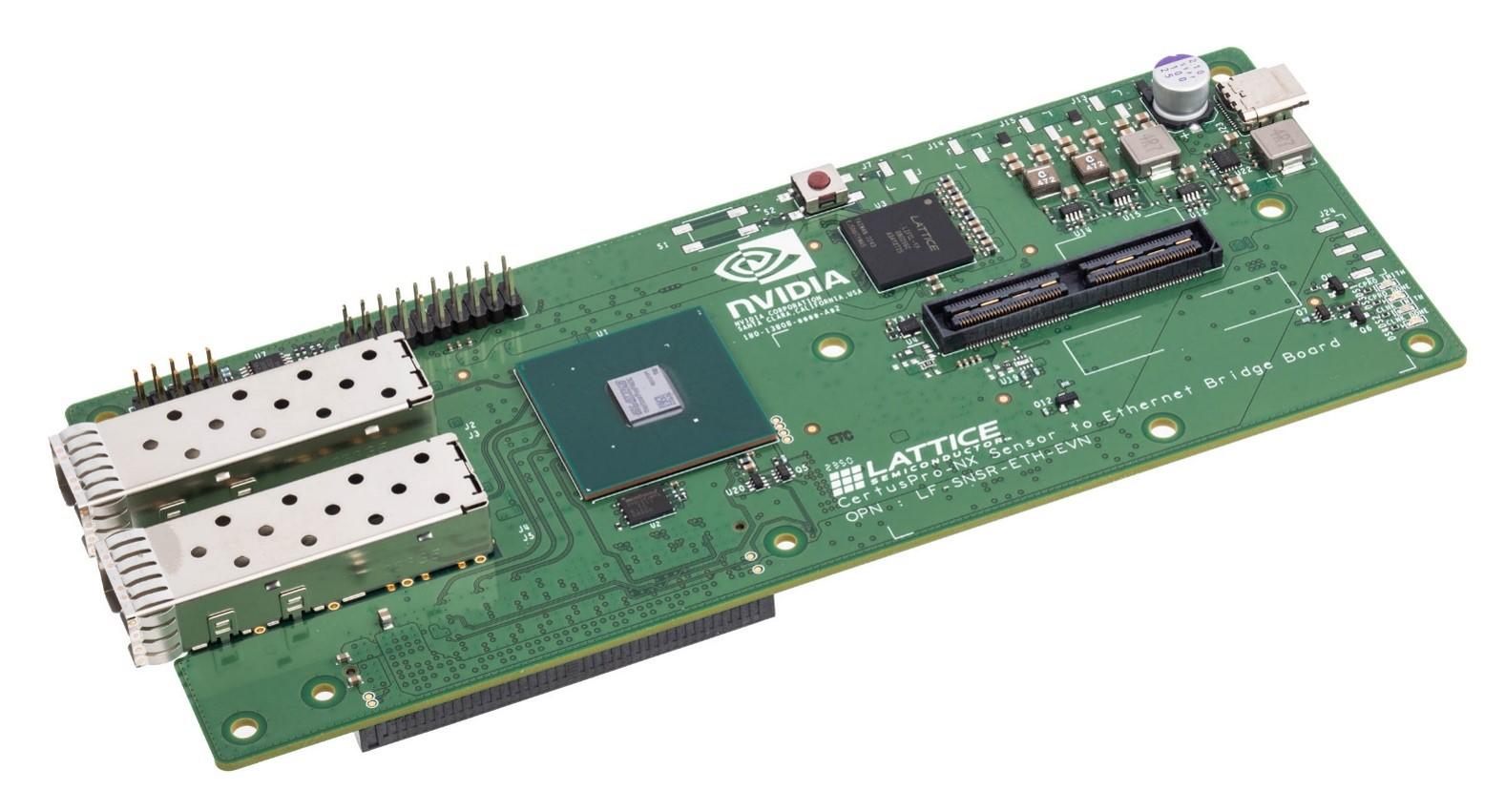
This board is an evaluation board that we would like to recommend to anyone considering implementing smooth data transmission from sensors to a GPU when performing edge computing processing using various sensor data.
This is particularly useful when image sensor data needs to be input into the GPU for image recognition using edge AI.
It is intended to act as a bridge between an image sensor with a MIPI interface and an NVIDIA GPU (IGX Orin, AGX OrinGPU).
When it is necessary to perform some kind of processing using a GPU in an edge environment, the following issues may arise.
- The physical space is small, so the GPU cannot be placed close to the image sensor.
・The GPU cannot be placed close to the image sensor because it cannot supply enough power.
・It would be too costly to allocate a GPU for each sensor, so we want to aggregate some sensor data and send it to the GPU.
・The sensor and GPU must be placed at least several tens of meters apart
The MIPI D-PHY I/F is an I/F standard that was originally developed for the purpose of standardizing the internal interfaces of mobile products. As such, it is generally intended for use for transmissions of up to a few tens of centimeters at most, making it an unsuitable means of communication for long-distance transmissions.
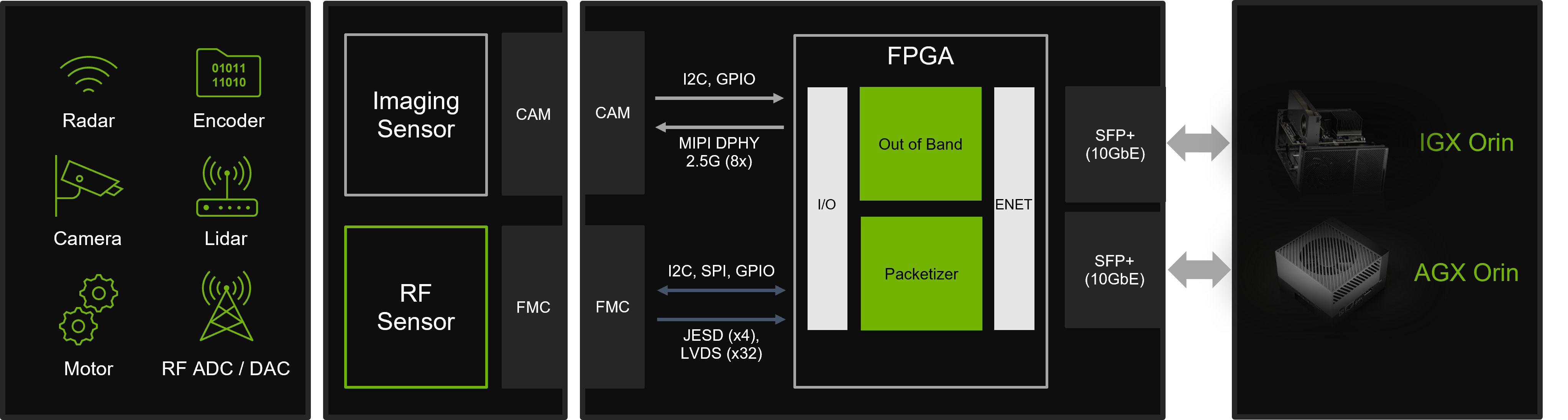
Therefore, this reference board converts the sensor's MIPI CSI-2 to 10Gbps Ethernet on the FPGA, providing an environment that enables long-distance communication between the sensor and the GPU.
Long distance transmission using interface bridge
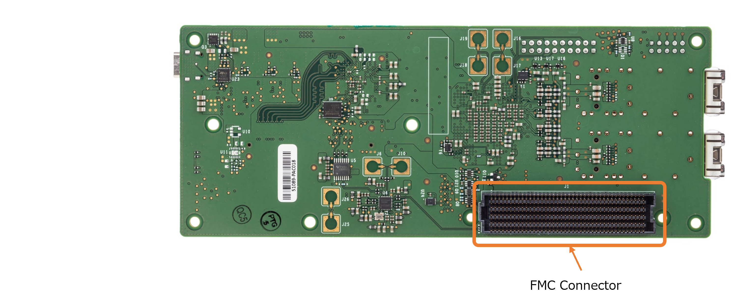
The evaluation board has the following connectors:
・Camera Connector
・10Gb Ethernet SFP+ Port
・FMC Connector
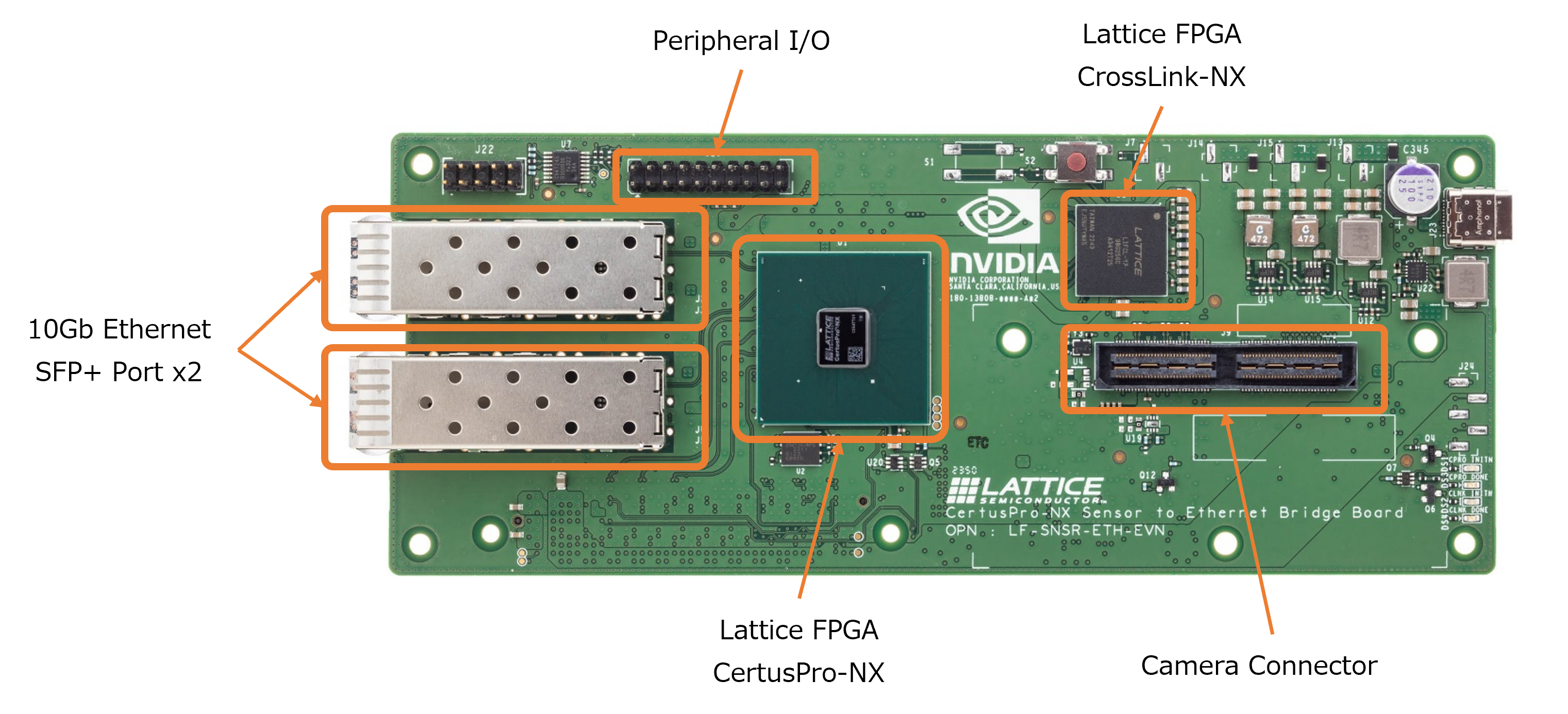
The Camera Connector can be connected to the Leopard Imaging LI-JETSON-IMX274 Dual Camera Module.
This Camera Module is equipped with Sony's IMX274 image sensor, which outputs images via MIPI CSI-2.
It also has two SFP+ ports, and by connecting an SFP+ adapter to these ports, you can connect over long distances to NVIDIA AGX Orin or IGX Orin using a Cat6 Ethernet cable or fiber optic cable.
FPGA used: Lattice Nexus series
The evaluation board is equipped with two FPGAs, each of which has the following roles:
CrossLink-NX: MIPI CSI-2 reception from image sensor and data transmission to downstream FPGA
CertusPro-NX: Receives data from the previous FPGA (CrossLink-NX), packets it to Ethernet UDP using Hololink FPGA IP, and transmits Ethernet data using the SerDes block
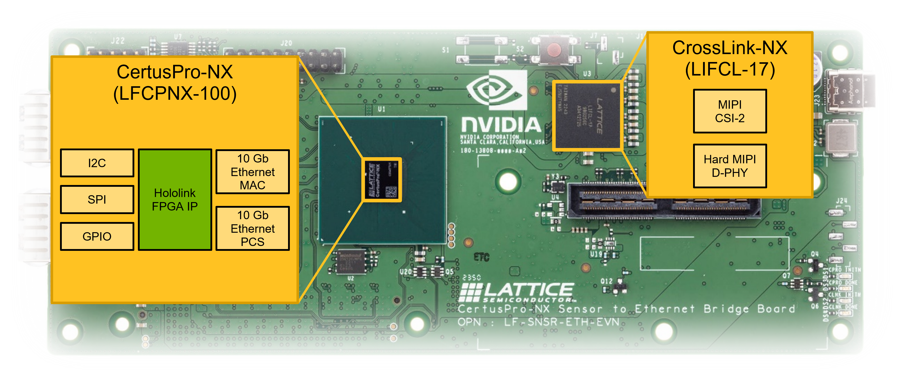
CrossLink-NX has a built-in MIPI D-PHY hard macro and is equipped with 8 lanes (= 4 lanes x 2ch) of I/O that can transmit MIPI data at up to 2.5Gbps/lane. It also supports high-speed differential I/F such as LVDS and SLVS, and is an FPGA that can receive images from high-speed MIPI output sensors and convert them to different I/Fs.
On the other hand, CertusPro-NX not only supports high-speed differential I/F, but also has an even faster clock-embedded data transmission block (SerDes) that can transmit at up to 10Gbps/Lane, so it receives sensor data transferred from CrossLink-NX and converts it to 10Gbps Ethernet for transmission. Hololink FPGA IP is also implemented in CertusPro-NX, which realizes high-speed, low-latency data communication with NVIDIA GPUs, and performs protocol conversion and data path optimization between GPUs and FPGAs. It is used for applications such as image processing and machine learning.
The Lattice Nexus series of FPGAs have the following features, making them ideal devices for a variety of edge applications:
- The FD-SOI process is used, and the device consumes approximately 1/4 the power of other companies' FPGAs of the same size.
As a result, the device generates very little heat, reducing the cost of heat countermeasures for the entire board.
- We offer a lineup of extremely small packages, which means that you can use devices that are approximately 1/6 the size of other companies' FPGAs in the same scale.
Summary
We have explained cases where long-distance transmission is required while using the MIPI interface.
Recently, the use of AI, including ChatGPT, has been increasing rapidly, and with the commoditization of cloud AI, it is expected that the use of AI on the edge side will also increase in the future. I believe that the content introduced here will lower the hurdle for using GPUs on the edge side and contribute to faster environment construction.
We hope that this information will be helpful in your consideration and development.
Inquiry
If you have any further questions or need more information about this evaluation board, please feel free to contact us!