- Semiconductor BusinessHOME
- Products and Services of Macnica,Inc.
-
technical information

-
Events and Seminars
- Handling Manufacturer
- Support
- Inquiry
- Click here to purchase products
- Semiconductor business e-mail magazine registration
![]()
![]() Narrow down by specifying conditions
Narrow down by specifying conditions
現在2189件がヒットしています。check

hello.
My name is Hanako Altera and I provide technical support for Altera® FPGA products at Macnica.

If you are a hardware engineer or system engineer in this era, you have probably heard of a semiconductor device called FPGA (FPGA) at least once. FPGAs are familiar to us, but any product will always have a “first-timer”. People who say "I'm going to start FPGA from now on!" still need study, knowledge, and information research.
The theme is "What is an FPGA?", but I won't write the general basic knowledge of FPGA here! A web search for “what is an FPGA” now yields a wealth of information. So I'll leave the general basic knowledge to you... Here, I would like to send out a little more broken information.
(By the way, I'll just write this down.)
In a nutshell, FPGAs are "logic devices whose circuits can be rewritten later."
The word FPGA is an acronym for Field Programmable Gate Array. It means semi-custom LSI ].
by the way,
CPLD is a non-volatile IC whose etymology is Complex Programmable Logic Device.
Both are attractive because they are programmable.
How big is your device?
In short, the range is huge. With such a wide variety of devices available, developers can purchase devices of the appropriate size (capacity) and keep their budget low.
Before we give specific numbers for device scale, let's talk a bit about units of scale.
FPGAs have a unit of measurement to express the size (capacity) of the device, and users use this as a guide when selecting a device. Currently, this unit is not standardized among manufacturers. For example, Altera® FPGAs call it logic element (LE), while Xilinx calls it logic cell (LC), and lattice indicates the number of LUTs (look up tables) it has. Incidentally, an LUT is the core part of the logic circuit block of an LE or LC. (For more information, do a web search. There is a lot of information available.)
Although the basic principle of LUT is the same among FPGA manufacturers, the number of LEs and LCs is not equal because the details of the structure are slightly different. I can't strictly compare LE and LC, but roughly speaking, they are almost equal, so I think you can use it as a guideline.
Now let's get back to it.
Altera® FPGAs feature LEs ranging from 40 small ones to 10,200K large ones (as of July 2026). In terms of ASIC gates, 1 LE is equivalent to approximately 12 gates.
that's why
10,200 KLE x approximately 12 = equivalent to 122,400 K gates
This can be estimated.
But actually, this is not the logic circuit scale that FPGA can realize! FPGAs now have a variety of blocks such as DSP (multiplier) blocks, memory, PLL, transceiver, ARM, etc. in addition to LE, so it is difficult to simply convert it to gates. Well, as a minimum guideline, I think it is good to estimate by adding up the number of LEs and the maximum number of 18x18-bit multipliers.
For example, a 5,510K LE FPGA might have 3,960 18x18 bit multipliers.
An 18x18 bit multiplier is calculated as approximately 5,000 gates.
3,960 x approximately 5,000 = 19,800K gate equivalent
Since LE has approximately 66,120K gates, the FPGA model number can be converted to ASIC gates.
66,120K + 19,800K = Equivalent to an 85,920K gate.
This can be estimated.
Furthermore, it has dedicated blocks for internal memory, PLL, transceivers, etc.
Equivalent to 85,920K gate + α
That's how it works.
Internal memory (excluding MAX® II and MAX® V) ranges from a minimum of 108 Kbit to a maximum of 410 Mbit.
User I/O pins range from a minimum of 27 pins (36-pin VBGA package) to a maximum of 1,640 pins (2,912-pin FBGA package).
The product lineup varies depending on the FPGA series, so please consult the manufacturer's handbook, also known as the datasheet. (This information is current as of July 2026. Product information for pre-release items may change.)
When actually designing a circuit, it's often difficult to utilize 100% of the target device's capacity (resources). If you use every block to its fullest extent, the wiring connecting each block will become congested, making it impossible to achieve the desired device speed, or in the worst case, making placement and routing impossible. Furthermore, without unused resources, it becomes difficult to accommodate changes in the circuit (specifications). To ensure flexibility, it is recommended to select devices with a capacity that will initially result in a device capacity (resource) utilization rate of approximately 80% or less for logic circuits.
What is the operating speed?
The internal operating speed of an FPGA can reach around 200MHz if the resources used by the logic circuits are kept below 80% and the clock control method for data transfer within the FPGA is configured to be synchronous (flip-flops operating at the same clock). Furthermore, with the latest FPGAs, it's possible to use around 90% of the resources, making operation at over 500MHz realistic. Of course, it also depends on how the user designs their circuitry, and in some cases, it may not even reach 100MHz. In short, the internal operating speed of an FPGA depends on the design and configuration of the user's logic circuits.
While 500MHz might sound slow to software designers, FPGAs are hardware, so parallel processing is a breeze for them! Furthermore, because the hardware can be freely designed, you can further increase processing power (throughput) by optimizing how data is processed.
FPGAs offer high external operating speeds thanks to their internal transceiver blocks and support for a wide variety of I/O standards, including DDR4/DDR5 SDRAM, PCI Express (PCIe), Serial RapidIO, and Gigabit Ethernet. The latest FPGAs achieve data transfer speeds of up to 116 Gbps. (This information is current as of July 2026. Product information prior to release may change.)
What are the development costs?
Developing an FPGA or CPLD roughly costs something like this.
| development cost | For FPGAs and CPLDs... |
| Labor costs required for design and verification | ⇒ 自社で開発すれば、人件費は抑えられます。 |
| Development environment (software) | ⇒ Use Quartus® Prime Lite Edition for 0 yen! |
| device | ⇒ Inexpensive ones can be purchased from the 100 yen range. |
| Mask and wafer manufacturing costs | ⇒ Not required. |
| Board design, device mounting | ⇒ The cost will vary depending on what kind of board specifications you use and whether you outsource or do it in-house. |
| write data | ⇒ You write the data yourself. In other words, the writing work costs 0 yen. However, if you do not have an Altera® FPGA download cable for writing, you will need to purchase one. |
| Design change of logic circuit | ⇒ (If you design it yourself) you can change it on the spot. (Because it's your own work) There is no additional cost. |
[Supplementary information regarding data writing]
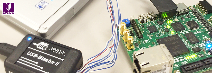
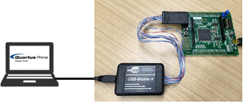
The FPGA is programmed while mounted on the circuit board. The FPGA has dedicated pins for programming, and these pins are wired to a connector provided on the circuit board. A dedicated download cable called USB-Blaster™ II or USB-Blaster™ III is used to connect the PC and the circuit board (connector). The Quartus® Prime programming utility (Programmer) is used from the PC to transfer data from the PC to the FPGA on the circuit board and program it. However, the FPGA is SRAM. For commercialization, it is also necessary to implement non-volatile memory (dedicated ROM or flash memory) on the circuit board to store the FPGA data.
What is the minimum purchase unit?
You can purchase from 1 piece!
Therefore, it can be used for any application that suits the user, whether it is for prototyping or for mass production.