- Semiconductor BusinessHOME
- Products and Services of Macnica,Inc.
-
technical information

-
Events and Seminars
- Handling Manufacturer
- Support
- Inquiry
- Click here to purchase products
- Semiconductor business e-mail magazine registration
![]()
![]() Narrow down by specifying conditions
Narrow down by specifying conditions
現在2149件がヒットしています。check
What is CoolSiC™?
CoolSiC™ is Infineon's proprietary SiC technologyIt is a trademark.
Infineon has more than 25 years of experience in developing SiC products since 1992, and has a proven track record of adoption in a wide range of applications, including automotive, industrial, and consumer products.
To this end, the company is investing heavily in expanding its own front-end factories, making it an extremely strong manufacturer in terms of BCM as well.
This page introduces the latest CoolSiC™ G2 technology, but please also refer to our other pages which introduce previously released CoolSiC™ products.
Related article
CoolSiC™ G2 Technology
CoolSiC™ G1 technology was first introduced in 2017 and has several features that give it competitive performance: Robust and reliable, CoolSiC™ G1 technology features a wide gate voltage (VGS) range, a high threshold voltage (Vth) to prevent parasitic turn-on even with a gate turn-off voltage of 0V and robust body diode behavior even under hard commutation.
Additionally, to reduce stress and strain on the SiC chip that could lead to delamination of the chip from the leadframe, CoolSiC™ G1 and G2 technology uses Infineon's proprietary XT package interconnect technology, which provides an extremely robust chip attachment via diffusion soldering, improving reliability as well as Rth.
The G2 technology, announced in early 2025, is based on the G1 technology, but the price/performance ratio is improved by shrinking the cells, and several additional features improve the core functions of the device. The lineup has now been expanded to include 750V rated devices for automotive, industrial and consumer use.
feature
- Reduces power loss by approximately 5 to 20% under typical load conditions
- Improved XT technology reduces RthJC by 12%
- Wide maximum transient VGS range of -10V to +25V
- Very low defect rate maintains the high reliability of G1 technology
- 750V lineup with top-side cooling package for excellent heat dissipation
Top-side cooling package
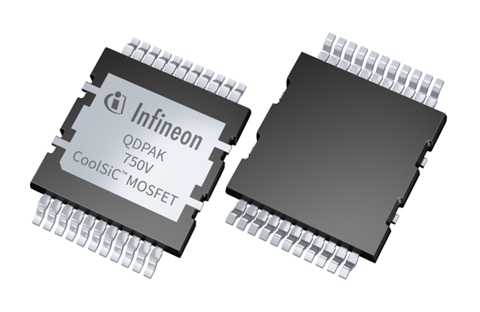
The CoolSiC™ 750V G2 series lineup is scheduled to be expanded in due course, but the top-side cooling QDPAK package product has already been released.
Top-side cooled QDPAKs can reduce thermal resistance by up to 35% over standard bottom-side cooling. By allowing the use of both sides of the PCB, top-side cooled packages utilize board space more efficiently and can achieve at least twice the power density. In addition, the thermal resistance of the leads is much higher than if the top of the package was exposed, so the thermal management of the package is improved by thermal decoupling from the board.
In addition, compared to combining FR4 and IMS, all components can be covered with a single sheet of FR4, and fewer connectors are required, which leads to a reduction in overall bill of materials (BOM) costs. QDPAK is also registered as a JEDEC standard, so you can use it with peace of mind in terms of reliability.
application
- On-board charger (OBC)
- DC-DC converter
- Ancillary Equipment for Electric Vehicles (xEV)
- e-fuse
- EV charging
- storage system
- communication
- SMPS
- solar inverter
Inquiry / Quotation
If you have any questions or would like a quote regarding this product, please contact us below.
Infineon manufacturer information TOP
Please return to the Infineon manufacturer information TOP page below.