- Semiconductor BusinessHOME
- Products and Services of Macnica,Inc.
-
technical information

-
Events and Seminars
- Handling Manufacturer
- Support
- Inquiry
- Click here to purchase products
- Semiconductor business e-mail magazine registration
![]()
![]() Narrow down by specifying conditions
Narrow down by specifying conditions
現在2004件がヒットしています。check

Overview
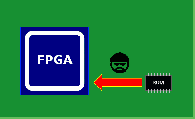
Design security features are provided to protect designs and intellectual property (IP) implemented within FPGAs from duplication, reverse engineering, and tampering.
Mechanism of design security
Encrypting the configuration data with an AES (Advanced Encryption Standard) key makes the configuration data unreadable even if it is intercepted.
The FPGA boots after decrypting the encrypted configuration data with the AES key inside the FPGA.
This method of using the same key for encryption and decryption is called "common key cryptography".
Since the AES key is the most important part of this mechanism, it is not possible to remove/delete/modify the AES key from the FPGA.
Encryption work and boot flow
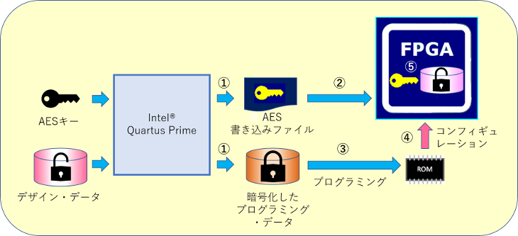
1. Generate write file
Input your design data and any AES key into Quartus ® Prime and it will generate an “AES write file (.ekp)” and “encrypted programming data”.
2. Write AES key to FPGA
1. Write the “AES write file” generated in step to the FPGA. This is the key to decrypt the "encrypted configuration data".
3. programming
1. Writes the "encrypted programming data" generated in , to an external configuration ROM or flash memory. The writing method is the same as writing normal programming data.
4. configuration
When the FPGA with the AES key written to it boots up, it reads "encrypted configuration data" from an external ROM.
5. Restore and boot
The AES key (AES write file) inside the FPGA and the decryption circuit automatically restore the "encrypted configuration data" to the original configuration data before booting.
Other encrypted programming data can be used with the same FPFA as long as the AES key is the same.
Glossary
The name of the data changes depending on the usage, so we will explain it to avoid confusion.
| design data | : Circuit design data such as RTL |
| programming data | : Data to write to ROM for configuration |
| configuration data | : Data to write to FPGA |
2 AES keys
There are two types of AES keys: volatile and non-volatile.
Both strongly prevent duplication, reverse engineering, and unauthorized tampering.
AES key that can be handled by FPGA
FPGAs can use volatile or non-volatile AES keys.
・Volatile key
The volatile key saves the AES key in volatile (data disappears without power) SRAM memory built into the FPGA.
The AES key can be changed or deleted, but the AES key will be lost unless the data is always backed up with an external power supply.
Volatile AES keys are useful for protecting configuration data during prototyping.
・Non-volatile key
Non-volatile key stores the AES key in a fused non-volatile key built into the FPGA.
Writing the AES key physically blows the fuse, so no external power backup is required and once written, the AES key cannot be changed or erased.
Even the manufacturer will not be able to analyze the failure of the FPGA, and JTAG will not accept any instructions other than 1149.1/1149.6 (JTAG Boundary scan test ).
Non-volatile keys are highly secure and help protect “production configuration data”.
| Key type | key length | change or delete | External power supply | Key writing method | Recommended |
| volatile key | 256bit | Possible | requirement | on board | Trial production |
| non-volatile key | 256bit | impossible | unnecessary | on board/off board | mass production |
AES key for CPLD (MAX® 10)
You can store the AES key in the MAX ® 10's internal non-volatile flash ROM. Because it is flash ROM, it can be modified and erased, and does not require an external power supply to store the data.
The MAX ® 10 does not have a non-volatile key with a fuse.
| Key type | key length | change or delete | External power supply | Key writing method | Recommended |
| non-volatile key | 128bit | Possible | unnecessary | on board/off board | Prototype & mass production |
How to write AES key
There are two ways to write the AES key: on-board and off-board.
on board
On-board is a method of writing the AES key to the FPGA device mounted on the board via a cable, etc.
You need a terminal to connect the cable on the board, but you can write it yourself.
off board
Off-board is a method of writing the AES key directly to the FPGA before implementation.
Since it uses a dedicated programmer, it is characterized by high writing reliability and fast writing speed.
However, it is expensive because it requires a socket (adapter) to connect the programming programmer and FPGA.
Macnica 's programming center has multiple programmers that can write AES keys, and has a rich track record of writing AES keys.
If you would like to write an AES key at Macnica, please feel free to contact us.
| writing method | writing tools | Optimal write quantity |
| on board | JTAG/Ethernet Blaster/USB-Blaster etc. | Few to medium |
| off board | write-only programmer | medium to large |
For MAX ® 10, the AES key and encrypted configuration data can be written to the device together or separately.
You can write AES keys to MAX ® 10 on-board or off-board with the same operations as in normal non-encrypted configurations.
How to keep the non-volatile key outside the FPGA
For those concerned about writing a one-time non-volatile key to the FPGA, there is a way to keep the non-volatile AES key off the FPGA.
Design Gateway's "IP Lock" is a solution that implements an AES-dedicated "encryption processing chip" on the board and decrypts the configuration data with a "decompression circuit" in the FPGA.
This "encryption processing chip" is a one-time key that cannot be changed or erased, but it is "small" and "cheap".
If you fail to write the AES key or change the key, you can replace the "cheap" cryptographic chip, which is less risky than replacing the FPGA. "IP Lock" is recommended for high-end and expensive FPGA encryption.
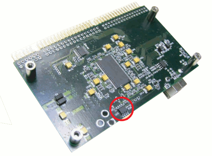
<Encryption processing chip mounted on board (red circle)>
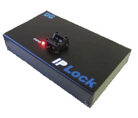
<IP Lock Writer>
Advantages of IP Lock
・Protect with 128bit AES key + 32bit product ID!
・Encryption processing chip and IP Lock writer are also authenticated as product ID!
・The authentication data is changed and encrypted at a cycle of about 5 times per second!
・Small and inexpensive dedicated cryptographic processing chip!
・We have a dedicated writing machine "IP Lock Writer" that is inexpensive and highly reliable for mass production!
・There is no need to purchase a large socket (adapter) for each type of FPGA!
・Products from reliable domestic suppliers. There is generous support in Japanese!
IP Lock Constraints
IP Lock puts the AES key outside the FPGA, so there are some restrictions.
・You can only write the AES key to the cryptographic processing chip once, and if you fail to change or write the key, you will need to replace the cryptographic processing chip.
・Necessary to write the AES key to the encryption processing chip (can be contracted)
・An area to place the encryption processing chip (SOIC-8) and wiring (2 wires) are required on the board in advance.
・Requires AES recovery circuit (1.3K LE + 25K bit mem) in user logic
laboratories pack
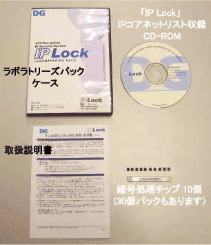
For trial purposes, we have prepared a "lavatory pack" that contains 10 encryption processing chips with AES keys embedded in advance, a recovery circuit for each AES key, and a Japanese manual.
The AES key and recovery circuit are paired, and each pack has a different AES key.