- Semiconductor BusinessHOME
- Products and Services of Macnica,Inc.
-
technical information

-
Events and Seminars
- Handling Manufacturer
- Support
- Inquiry
- Click here to purchase products
- Semiconductor business e-mail magazine registration
![]()
![]() Narrow down by specifying conditions
Narrow down by specifying conditions
現在2162件がヒットしています。check

This article will explain the basics of linear regulators and LDOs. This time, we will use the Analog Devices ADP1715 datasheet as a reference to explain the output voltage settings and errors of common linear regulators and LDOs.
*This article includes the datasheet as well as the first half of Section 1 of Practical Power Solutions.
CMOS Linear Regulator ADP1715
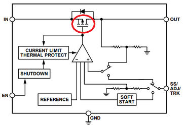
The ADP1715 is a CMOS linear regulator with an input voltage range of 2.5 to 5.5 V and an output current of 500 mA. It is called a CMOS linear regulator because it uses a CMOS as the internal power element, as shown in the red circle in Figure 1.
The advantages of using CMOS include the ability to reduce the dropout voltage (the difference between the input voltage and the output voltage) and the ability to develop and provide customers with products with reduced bias (self-consumption) current flowing to GND.
I will explain in detail in future articles the benefits of using CMOS, such as small dropout voltage and bias current.
Output voltage setting
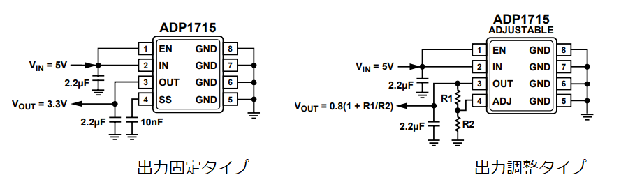
Regulator voltage settings are generally made using two voltage-dividing resistors. Other options include fixed-output products with all resistors built in, products that require only one external resistor, or products that use an internal register.
The ADP1715 is available in two versions: one with a built-in resistor for a fixed output, and one with an adjustable output using two external resistors.
Whether it is better to use an internal output setting resistor or an external resistor will be explained after an explanation of output voltage error.
Output voltage setting method
The output voltage is set by the voltage divider resistors R1 and R2 shown in Figure 2.
The datasheet states, "The maximum bias current to the ADJ pin is 100 nA, so to keep the error due to the bias current to less than 0.5%, use a value of less than 60 kΩ for R2." Therefore, select a resistance value of less than 60 kΩ for R2.
As such, it is important to note that the data sheet may contain comments about the resistance value to be selected. Even if there are no comments, it is recommended to select a resistance value with the same number of digits as the value of the reference circuit in the data sheet or application note.
The calculation formula is as follows:
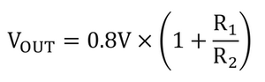
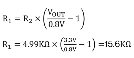
The 0.8V in this equation is the value of the internal reference voltage. R2 is set to 4.99KΩ based on the value on the demo board. To obtain an output voltage VOUT = 3.3V, the voltage divider resistor R1 is calculated as follows. When selecting a resistor with a 1% tolerance, it is selected from the E96 series, so in practice 15.4KΩ or 15.8KΩ is selected for R1.
Output voltage error
The output voltage error is determined by the sum of the following:
1. Variation in voltage divider resistors
2. Reference voltage variation
3. Line Regulation
4. Load regulation
When actually used in a system, it is possible to estimate the extent of the above variations based on the ambient temperature, input/output voltage conditions, and load current conditions. Depending on the accuracy of the estimated output voltage, it is possible to determine whether the power supply can be used as a power supply for the load microcontroller or FPGA.
1. Variation in voltage divider resistors
The output voltage error also occurs due to variations in the voltage divider resistors R1 and R2 used. When E96 series resistors are used, the error is ±1%.
Let's calculate the output voltage error when the output voltage setting is 3.333V (R1 = 15.8KΩ, R2 = 4.99KΩ). If the error of the two voltage divider resistors used is ±1%, the maximum error will be when R1 is +1% and R2 is -1%, so if we calculate the output voltage using equation 1, the output voltage will be 3.384V, which is an error of approximately 1.5% from the set voltage of 3.333V.
Because the variation in resistance value is ±1%, some people intuitively think that the output voltage has a maximum error of 2%, but when you actually do the calculation, you find that the error is not 2%. This shows how important it is to actually perform the calculation and check.
2. Reference voltage variation
The reference voltage may be referred to in various ways, such as feedback voltage, depending on the manufacturer and product, so please check the datasheet. In the datasheet for the ADP1715, it is referred to as "ADJUSTABLE OUTPUT VOLTAGE" (Table 1). Taking into account the load current and temperature range, this means that there is a maximum variation of 3%.

3. Line Regulation
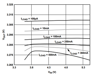
Line regulation specifies the variation in output voltage when the input voltage fluctuates. Referring to the electrical characteristics table (Table 2), the variation is ±1.5%/V.

The ADP1715 data sheet lists the line regulation when the output is set to 3.3V (Figure 3), so you can use this data as a reference to estimate variation. In applications with large input voltage fluctuations, it is also important to actually check the output voltage variation using similar data on an evaluation board, etc.
4. Load regulation
Load regulation specifies the variation in output voltage when the load current fluctuates. Referring to the electrical characteristics table (Table 3), the variation is ±0.004%/mA.

The ADP1715 data sheet lists load regulation when the output is set to 3.3V (Figure 4), so it is possible to estimate variation by referring to this data. In applications with large load current fluctuations, it is also important to actually check the output voltage variation using similar data on an evaluation board, etc.
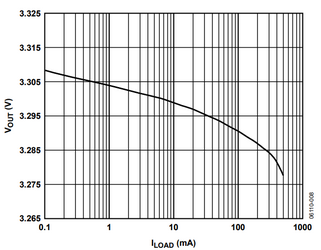
The load regulation characteristics in Figure 4 show that the output voltage drops as the load current increases. Because of these characteristics, there may be times when you want to adjust the output voltage.
There may also be cases where you want to adjust and set the output voltage taking into account temperature and deterioration over time. In such cases, if the voltage divider resistor that sets the output voltage is built in, it will not be possible to adjust it, so if you anticipate that the circuit you are designing will require output adjustment, it is safer to select a product with an external voltage divider resistor.
Click here for recommended seminars/workshops
If you would like to learn more about methods for estimating output voltage errors and the impact they have on digital circuits, as discussed in this technical article, please consider attending the "Basic Seminar on Power Supplies for Digital Circuit Designers" in the seminar list at the link below (held every 3-4 months).
Click here for recommended articles/materials
LTspice List of articles: Let's use LTspice series
FAQ regarding analog function IC: FAQ list
List of technical articles: technical articles
Manufacturer introduction page: Analog Devices, Inc.
List of articles on the basics of linear regulators
- Output voltage setting and error
Inquiry
If you have any questions regarding this article, please contact us below.
Analog Devices Manufacturer Information Top
Analog Devices Manufacturer Information If you would like to return to the top page, please click below.