- Semiconductor BusinessHOME
- Products and Services of Macnica,Inc.
-
technical information

-
Events and Seminars
- Handling Manufacturer
- Support
- Inquiry
- Click here to purchase products
- Semiconductor business e-mail magazine registration
![]()
![]() Narrow down by specifying conditions
Narrow down by specifying conditions
現在2185件がヒットしています。check

Newly released LT83401/2with 42Vin support
Switching regulators are noisy, so in circuits that are sensitive to noise, it is common to add an LDO after the regulator. However, adding an LDO reduces efficiency and increases the design burden. Have you ever thought, "If I had a low-noise switching regulator, I wouldn't need an LDO?"
In fact, Analog Devices offers an unprecedented ultra-low noise switching regulator, the Silent Switcher 3. This product is ideal for circuits that previously used LDOs as a noise countermeasure, or circuits that require low noise and high current.
Here we will introduce the features, benefits, and lineup of Silent Switcher 3.
Issues with switching power supplies
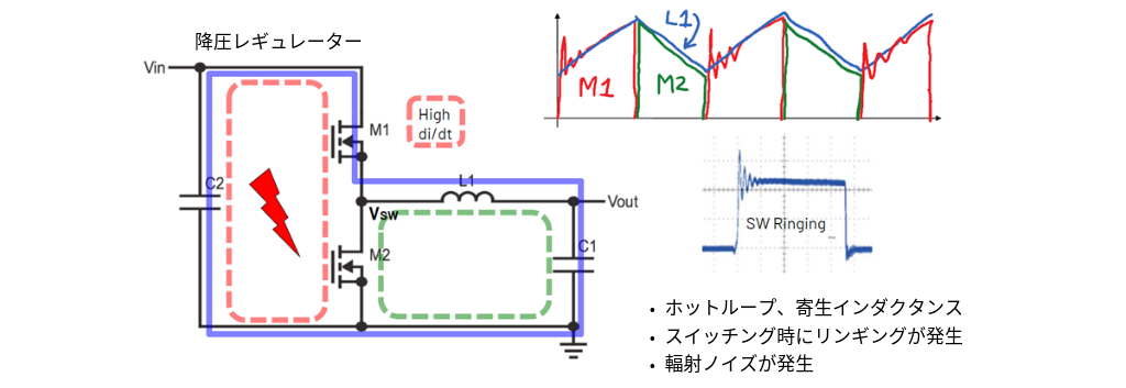
In general switching regulators, ringing occurs in the hot loop during switching operation, which causes noise. It is possible to use filters or mechanical shields to reduce noise, but this has the drawback of increasing costs and the board area.
Additionally, in noise-sensitive circuits, a common method of reducing noise is to add an LDO in the subsequent stage, but this brings issues such as heat generation from the IC, reduced efficiency, and an increased number of components.
Analog Devices' low-noise switching regulator, Silent Switcher 3, can solve these problems. It dramatically reduces low-frequency noise and can be used in noise-sensitive circuits without an LDO.
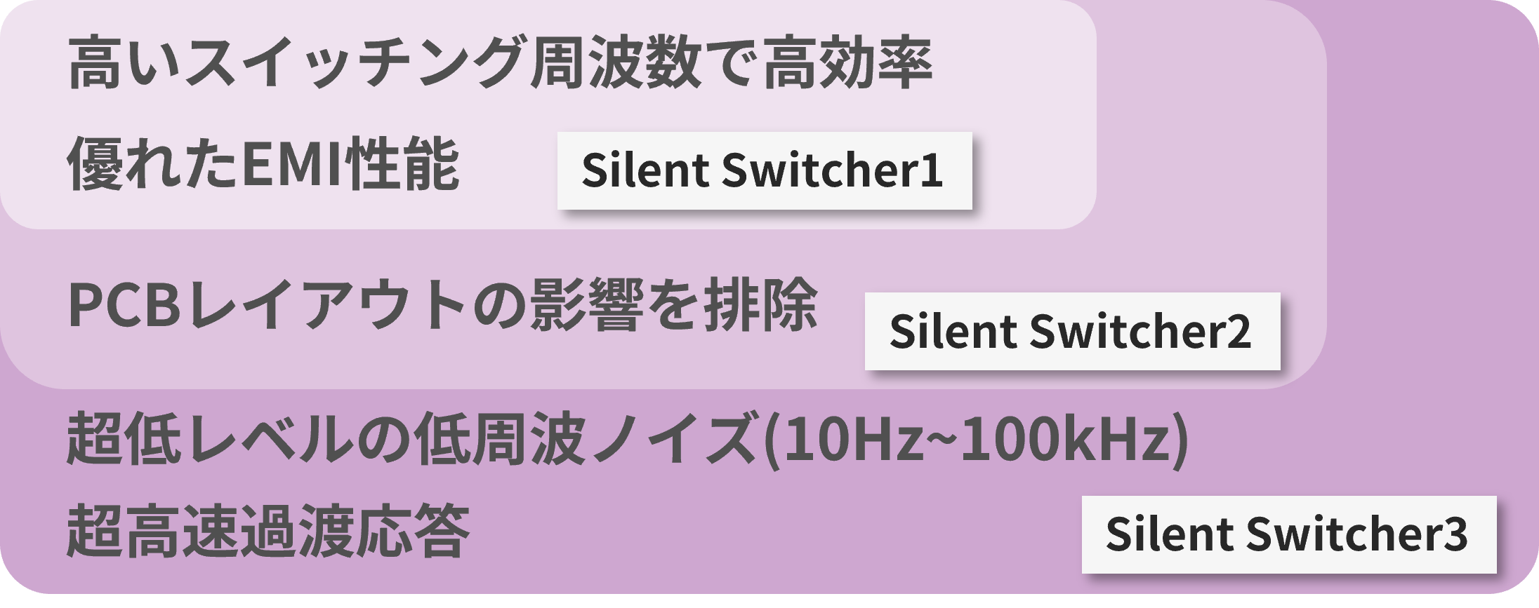
What is Silent Switcher?
"Silent Switcher" is Analog Devices' proprietary ultra-low noise DC-DC converter architecture that achieves "low EMI", "high efficiency", and "high switching frequency" without any trade-offs.
Silent Switcher Fundamentals
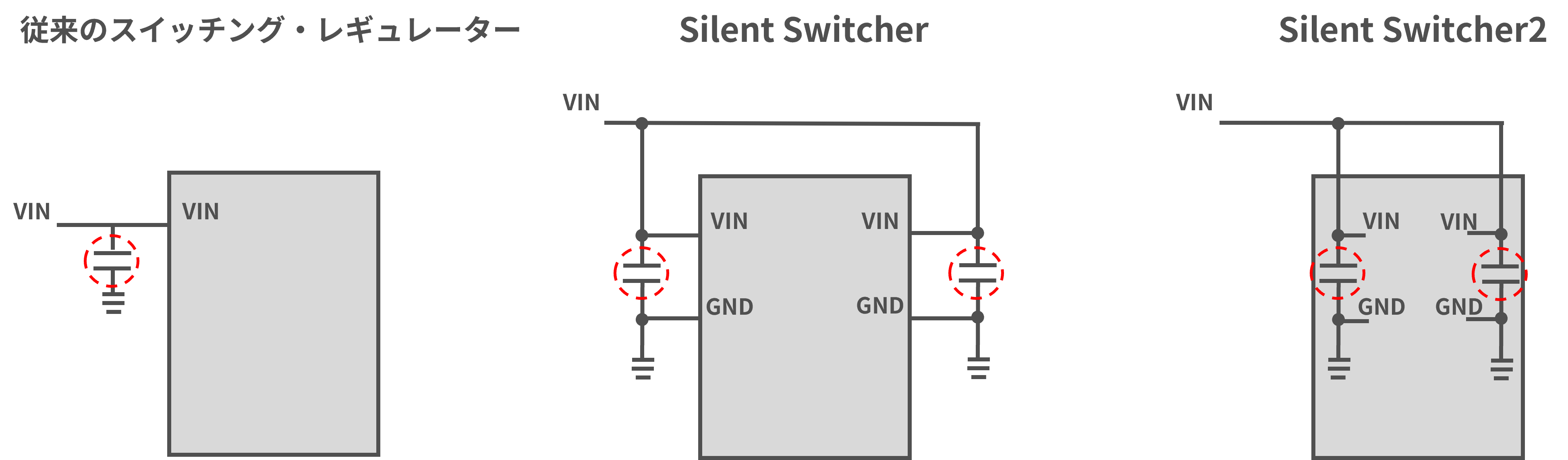
The first generation, Silent Switcher 1, features the following technologies:
・Bonding wire is changed to flip chip to suppress ringing
Silent Switcher minimizes parasitic L components by making wiring thicker and shorter!
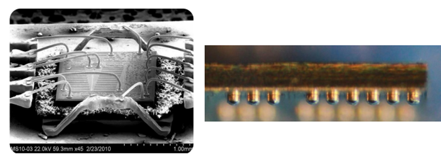
The bonding wires used in typical IC wiring are thin and long, which causes large parasitic inductance and ringing. Silent Switcher 1 does not use bonding wires and instead uses flip-chip connections. The thick and short copper pillars reduce parasitic inductance and suppress ringing.
・The hot loop was divided into two, successfully confining the magnetic field.
The magnetic field traps EMI noise.
The hot loop, which is the source of noise, is divided into two smaller loops and arranged to surround the IC, successfully containing the magnetic field and preventing the propagation of EMI.
・High efficiency even at high switching frequencies allows for smaller circuits
It features an internal switch driver that minimizes power loss during switching, resulting in fast and clean switching edges.
Silent Switcher complies with the most stringent noise standard, CISPR25 Class 5, and can solve the issues of noise, heat, efficiency, and size in power supply design all at once.
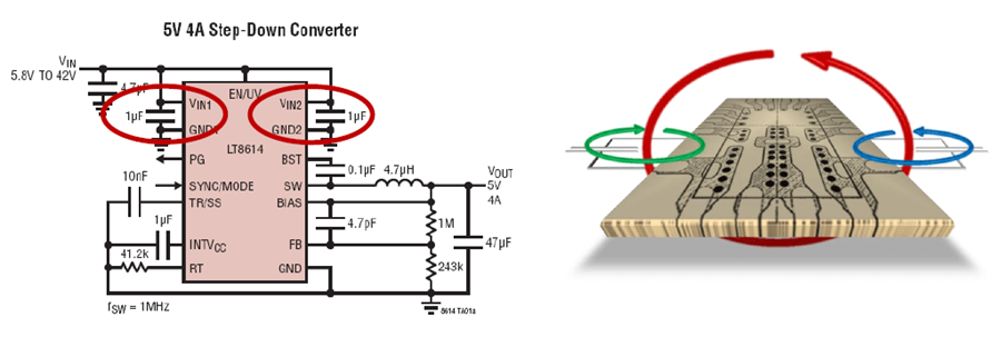
Silent Switcher 2
The second generation, Silent Switcher 2, has an input capacitor built into the package, eliminating the impact of PCB layout. Silent Switcher 1 required external capacitors to be placed symmetrically on both sides, but Silent Switcher 2 eliminates this constraint, allowing for a simpler, more space-saving design. In addition, the inclusion of an input capacitor makes the hot loop shorter, improving noise performance.
Silent Switcher 3
The third generation, Silent Switcher 3, achieves "reduction of low frequency noise (10Hz-100kHz)" and "ultra-fast transient response" in addition to the features of Silent Switcher 2.
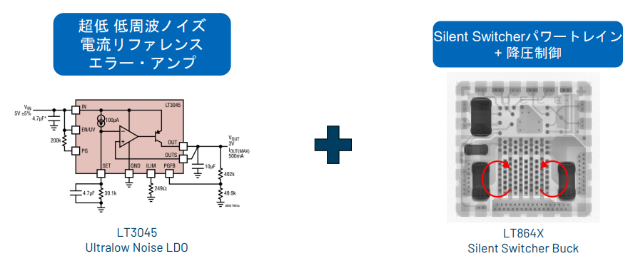
Silent Switcher 3 uses the current reference technology of Analog Devices' LT3045, the market's leading ultra-low noise LDO. By changing the conventional bandgap reference, which has a high noise component, to a current reference, we have succeeded in significantly reducing low-frequency noise. This allows the switching regulator to achieve noise performance comparable to that of an LDO.
Silent Switcher 3 Features
Specifically, what kind of noise characteristics does Silent Switcher 3 have? The table below compares the low-frequency noise from 10 Hz to 100 kHz of the Silent Switcher 3"LT8625S" with other solutions. The noise of the LT8625S is almost equivalent to that of a Li-ion battery, and is overwhelmingly lower than that of conventional LDOs.
| Integrated Noise from 10Hz-100kHz | |
| LT3045 (Industry's lowest noise LDO) | 0.8μVRMS |
| Lithium-ion battery | 2.7μVRMS |
| LT8625S (high bandwidth) | 2.7μVRMS |
| LT8625S (low bandwidth) | 3.7μVRMS |
| General low noise LDO | Approximately 4μV RMS |
| LT8643S (SS2 in unity gain fb) | 123μVRMS |
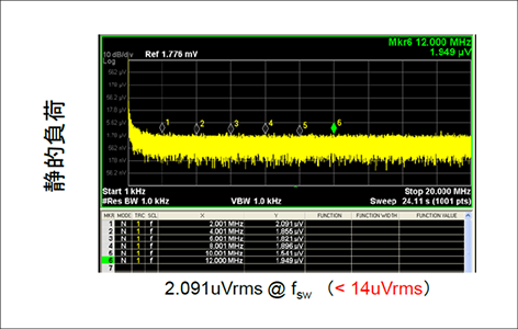
DCDC with lower noise than LDO and equivalent to battery
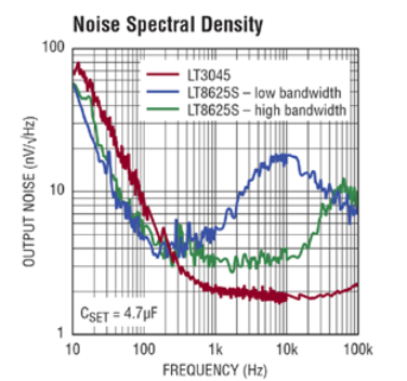
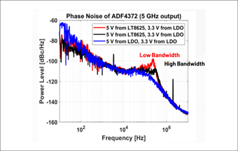
The figure on the right compares the noise spectral density of the LT8625S with that of the market-leading ultra-low noise LDO, the LT3045. Especially at low frequencies, the LT8625S has almost the same characteristics as the LT3045, and has superior noise performance.
・Can also be used for noise-sensitive RF power supplies
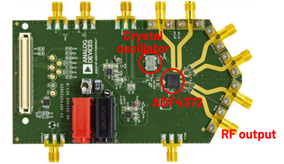
Evaluation board using Silent Switcher 3 (LT8625SP) for 5V power supply and LT3045 for 3.3V power supply
The Silent Switcher 3 's excellent noise characteristics allow it to be used in noise-sensitive circuits where switching regulators have traditionally been difficult to use.
For example, it was previously difficult to directly power a PLL device from a switching regulator. However, with Silent Switcher 3, you can achieve noise performance almost equivalent to that of the ultra-low noise LDO"LT3045" simply by adding an external second-stage LC post-filter. This makes it possible to use it as a GHz-band power supply for PLL devices and other devices.
The waveforms created using the LT3045 for both 5V and 3.3V are in blue.
When using the LT8625SP, some frequencies (several tens of kilohertz to several hundreds of kilohertz) deteriorate slightly.
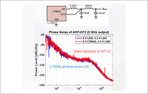
By adding an external LC post filter, the performance is almost equivalent to LT3045 x 2. It can also be used as a GHz band power supply!
*The LT3045isADI'slowest noiseLDO.
・No need for LDO, saving space and reducing costs
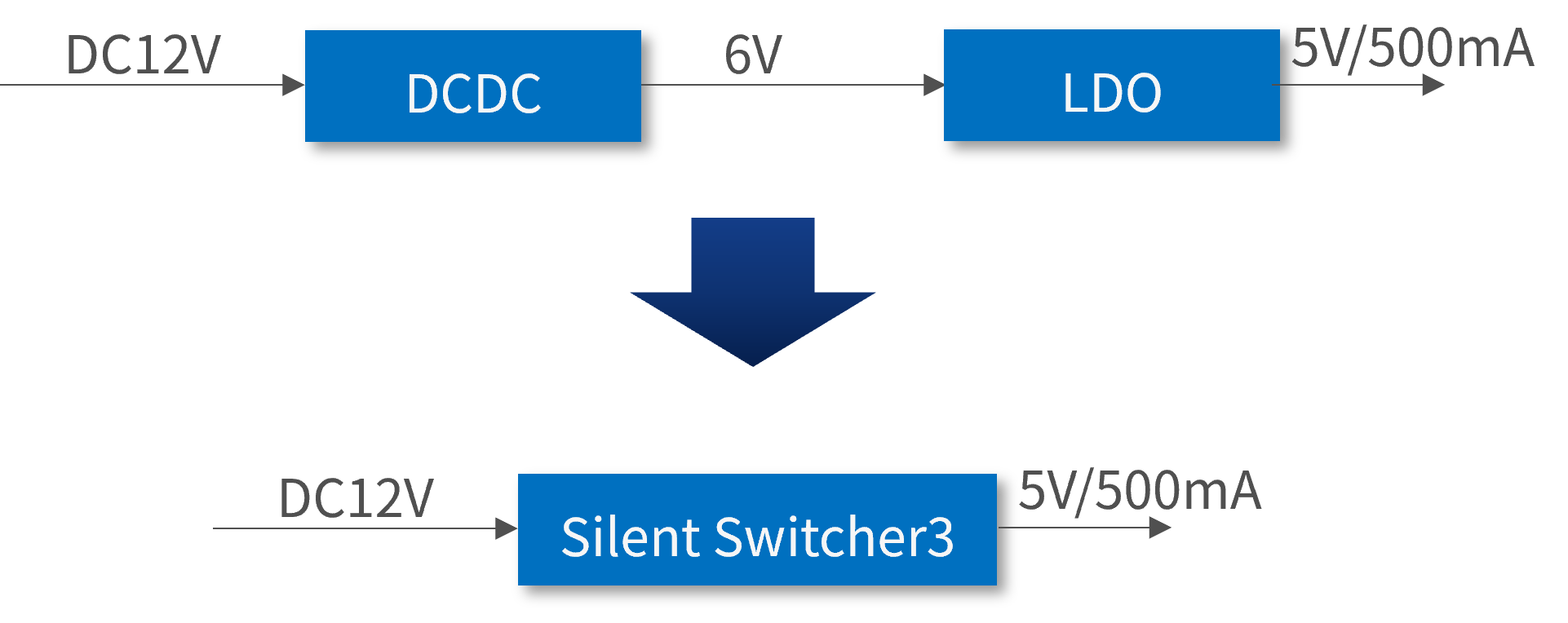
By using Silent Switcher 3, you can achieve a low-noise power supply without adding an LDO. For example, a circuit that was previously configured with two stages, such as "DC (12V) → DCDC (intermediate voltage 6V) → LDO (5V)", can be simply configured as "DC (12V) → Silent Switcher 3 (5V)".
Eliminating the need for an LDO reduces the number of components, simplifies the design, saves space, and reduces costs.
・Ideal for circuits that require low noise and high current
The Silent Switcher 3 is ideal for circuits requiring high current and low noise.
Due to the characteristics of LDOs, power loss is large at high currents, and heat generation becomes an issue. Conventionally, in high-current circuits that require low noise, it was necessary to use high-performance LDOs with good heat dissipation characteristics or to add an external heat sink, which increased costs and board area.
Silent Switcher 3 achieves both high efficiency and low noise, and suppresses temperature rise in ICs even at high currents. It also eliminates the need for an additional heat sink, contributing to reduced component count and space savings.
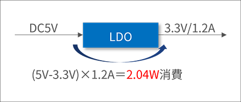
If you try to design with an ambient temperature of 40℃ and Tj=100℃ or less, then θjA×2.04W+40℃=100℃
θjA=(100-40)℃/2.04W=29.4℃/W
It is necessary to use an LDO that can handle large currents with good heat dissipation characteristics, or to implement a heat sink.
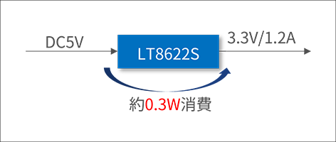
θjA=46℃/W
46℃/W×0.3W+40℃=53.8℃
There is a large margin for 100°C, so no heat sink is required!
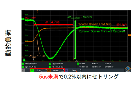
- Supports fast transient response, settling to within 0.2% in less than 5μs
The Silent Switcher 3 supports ultra-fast transient response, making it suitable for powering FPGAs, RF transceivers, and more.
Recent FPGAs and RF transceivers have increasingly stringent power supply requirements, and if the transient response is insufficient, there is a risk that the voltage will deviate from the specified value, resulting in malfunction.
The Silent Switcher 3 can settle to within 0.2 % in less than 5 μs, making it ideal for devices requiring fast transient response.
Silent Switcher 3 Lineup
The Silent Switcher 3 portfolio includes:
| model number | Vin (V) | Iout (A) | package | |
| LT83401 | 42 | 1 | 3×2 LFCSP | Pin compatible |
| LT83402 | 2.5 | |||
| LT83201 | 18 | 1 | ||
| LT83203 | 3 | |||
| LT83205 | 5 | |||
| LT8622S | 2 | 4×3 LQFN | Pin compatible | |
| LT8624S | 4 | |||
| LT8625S/SP | 8 | |||
| LT8625SP-1 | 8 | 4×4 LQFN | Pin compatible | |
| LT8627SP | 16 |
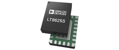
LT8625S LQFN Package
SP model: Optional heat sink attachment for high ambient temperature applications.
Possible Exposed Die Top Package (Exposed Pad on Top)
No heat sink is required to achieve the rated output current.
We have evaluation boards available for each product, so please give them a try.
This time, we introduced Analog Devices' switching regulator, "Silent Switcher 3," which achieves unprecedented low noise.
If you are interested, please feel free to contact us.
Application example
- Low Noise Instruments
- High speed/high precision ADC/DAC
- 5G Infrastructure Equipment
Click here to purchase products
Click here for manufacturer site/other related links
- Meets CISPR25 Class 5 requirements! Switching regulator that simplifies noise design for automotive ECUs
- LT8622S (Datasheets can be downloaded here)
- LT8624S (Datasheets can be downloaded here)
- LT8625S (Datasheets can be downloaded here)
- LT8627SP (Datasheets can be downloaded here)
- Three points for low-noise power supply circuit design
- LT83401 (Datasheets can be downloaded here)
- LT83201 (Datasheets can be downloaded here)
- LT83203 (Datasheets can be downloaded here)
- LT83205 (Datasheets can be downloaded here)
Inquiry
If you have any questions regarding this article, please contact us below.
Analog Devices Manufacturer Information Top
Analog Devices Manufacturer Information If you would like to return to the top page, please click below.