- 半導体事業HOME
- マクニカの製品・サービス
-
技術情報

-
イベント・セミナー
- 取扱メーカー
- サポート
- お問い合わせ
- 製品購入はこちら
- 半導体事業のメルマガ登録
![]()
![]() 条件を指定して絞り込む
条件を指定して絞り込む
現在2186件がヒットしています。check

正負電源を独立して制御可能なADP5072の特長
アナログ回路を設計する際に、CCDを含む各種センサ、オペアンプ、A/Dコンバーターなどプラスの電源だけでなくマイナスの電源が必要になる場合があります。
その際に1チップで正負電源が供給できるICを使用すると回路を小型化できるだけでなく、部品点数の削減によるコスト削減・信頼性向上に加え、設計工数の削減が可能になります。
この記事で正負電源IC ADP5072の以下の3つの大きな特長について解説します。
- 正電源と負電源を個別に調整/制御可能
- EMI/ノイズ対策も万全
- 正負電源でも小型・高効率
1. 正電源と負電源を個別に調整/制御可能
ADP5072の入力電圧範囲は2.85V ~ 5.5Vで、出力は正電源が最大35V/1A、負電源が-30V/0.6Aです。広範囲な出力電圧範囲はさまざまなアプリケーション向けの正負電源回路に適しています。
ADP5072の正電源と負電源を生成する内部回路は独立しており、それぞれを個別に設定することが可能です。
また、柔軟なスタートアップ・シーケンス機能を備えており、マニュアルでのイネーブル、同時モード、正電源優先もしくは負電源優先の調整が可能です。
以下はADP5072の内部回路図になります。

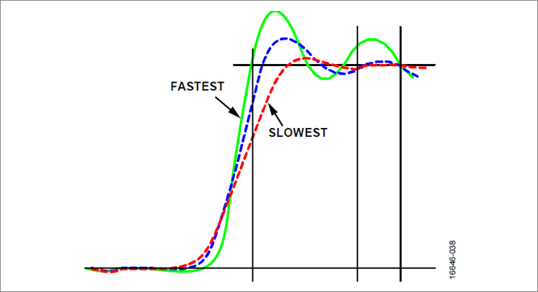
2. EMI・ノイズ対策も万全
ADP5072はプログラマブルなスルーレート制御回路を内蔵しています。
この回路は以下の図に示すようにスイッチングノードのスルーレートを低減します。
その結果、リンギングが低減し低EMIを実現します。
またADP5072は1.0 MHz〜2.6 MHzの外部発振器と同期できます。
この機能によりノイズに敏感なアプリケーションでノイズフィルタリングを容易になります。
3. 正負電源でも小型・高効率
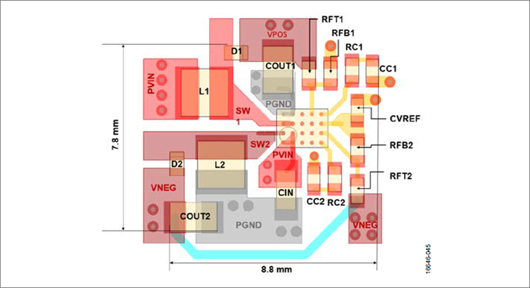
ADP5072のパッケージは1.61 mm x 2.18 mm WLCSPと小型で、スイッチング周波数は1.2MHzもしくは2.4MHzのため小さなインダクターが使用できます。このため、ADP5072は省スペースのアプリケーションにも適しています。
一例として、入力電圧N = 3.3 V、正電源 = 12 V/100 mA、負電源 = −3.2 V/60 mAの推奨レイアウトは7.8 mm x 8.8mmになります。
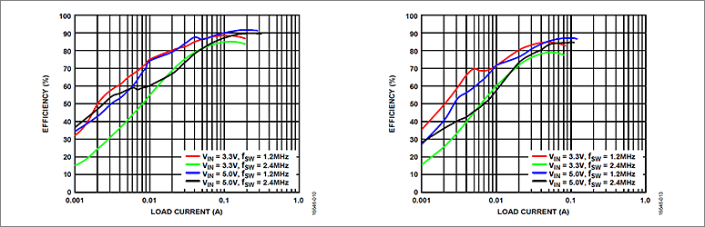
また、ADP5072は高効率なのでアプリケーションの低消費電力化にも貢献します。
アナログ・デバイセズの正負電源ICラインナップ
アナログ・デバイセズはADP5072の他にもさまざまな正負電源ICがリリースされています。
また、マイクロモジュールとLDOの組み合わせで正負電源を構成することも可能です。
詳しくは プラス・マイナス電源設計 をご参照してください。
|
入力電圧範囲 |
2.85V から 5.5V |
2.85V から 15V |
2.4V から 16V |
|---|---|---|---|
|
出力電圧 |
正電源 +35V 負電源 -30V |
正電源 +39V. 負電源 -39V |
正電源 +40V. 負電源 -40V |
|
出力電流 |
正電源 1.0A 負電源 0.6A |
ADP5070: 正電源 1.0A 負電源 0.6A ADP5071: 正電源 2.0A 負電源 1.2A |
正電源 0.9A 負電源 0.9A |
|
スルーレート制御 |
あり |
あり |
なし |
|
シーケンス制御 |
あり |
あり |
なし |
|
パッケージサイズ |
2.18 mm × 1.61 mm 20-ball WLCSP |
4mm x 4mm 20-lead LFCSP 20-lead TSSOP |
3mmx3mm 10-Lead DFN |
正負電源ICのラインナップ
アプリケーション例
- 正負電源の必要なオペアンプ、A/Dコンバーター、D/Aコンバーターなどの電源
- CCDのバイアス電源
- 光モジュール電源
- ToF (Time of Flight) モジュール電源
おすすめ記事/資料はこちら
商品の購入はこちら
メーカーサイト/その他関連リンクはこちら
お問い合わせ
本製品に関してご質問がありましたら、以下よりお問い合わせください。
アナログ・デバイセズ メーカー情報 Top へ
アナログ・デバイセズ メーカー情報 Top へ戻りたい方は以下をクリックしてください。