Site Search

Notes on Power Supply Sequence for FPGA (LDO Edition)

Many semiconductor devices, such as FPGAs, require multiple power supplies. Because they must adhere to a specific power supply sequence, they may require power on/off control pins and output capacitor discharge functions.

This time, I will focus on explaining four important points to keep in mind when using LDOs.

An on/off function is essential for creating a sequence

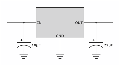
Modern FPGAs and DSPs commonly require power on/off sequences. To control these on/off states, the power supply IC (module) needs an enable pin for on/off control. Inexpensive LDOs may lack these on/off control pins, so careful selection is necessary.

Article header library 128077 pic01 1
Figure 1 : LDO without ON/OFF control

Rise time control

A soft-start function allows for control over the rise time. However, few LDOs have a soft-start function. As a workaround, it becomes necessary to control the rise time by adjusting the capacitance of the output capacitor. However, using a capacitor that is too large will cause problems during the fall-off phase.

Power down sequence

The specifications for the startup sequence are well known. However, the shutdown sequence has not received much attention until now. Recently, the number of power supplies mounted on a circuit board has increased, and if the shutdown sequence is not carefully considered, it can lead to a rush current flow. Therefore, it is important to pay close attention to the shutdown sequence as well.

For an explanation of why sequencing is necessary, please refer to this article.
Is power sequencing unnecessary?

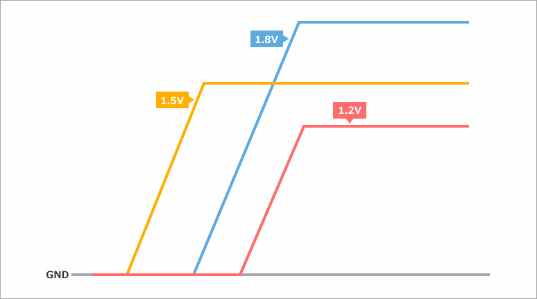
For the rise time sequence, increasing the output capacitor of the LDO is good from the perspective of lengthening the rise time, but it will lengthen the fall time (longer capacitor discharge time), which is disadvantageous for the fall time sequence, so caution is needed.

Article header library 128077 pic02 1
Figure 2 : Sequence diagram

LDO fall sequence

Switching regulators, if the low-side FET discharges when off, will cause the output voltage to drop quickly, making it easier to implement off-sequences. However, most LDOs lack a discharge function on the output side.

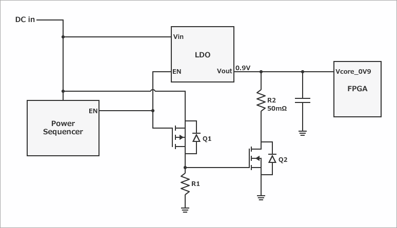
Therefore, controlling the startup sequence by increasing the output capacitor size is not recommended. If it becomes necessary, an external discharge circuit will need to be added.

Article header library 128077 pic03 1
Figure 3 : External discharge circuit

LDO with on/off function and discharge function

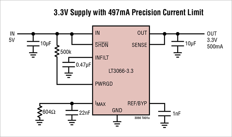
Analog Devices LDOs have an LDO like the LT3066 that has an on/off function (SHDN PIN in Figure 4) and a function to discharge the charge on the output section.

Article header library 128077 pic04 1
Figure 4: LT3066 schematic

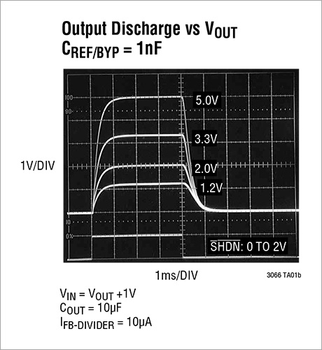
Figure 5 shows the waveform where the output voltage is quickly reduced to 0V due to the output discharge function.

Article header library 128077 pic05 1
Figure 5: Discharge characteristics

This functionality allows for the FPGA to perform the required power-down sequence while simultaneously supplying clean voltage to the PLL and analog power supply via LDO products.


Click here to purchase products

LT3066IMSEPBF
LT3061EMS8EPBF
LT3063IDCB

Inquiry

If you have any questions regarding this article, please contact us below.

Analog Devices Manufacturer Information Top

Analog Devices Manufacturer Information If you would like to return to the top page, please click below.