- 半導体事業HOME
- マクニカの製品・サービス
-
技術情報

-
イベント・セミナー
- 取扱メーカー
- サポート
- お問い合わせ
- 製品購入はこちら
- 半導体事業のメルマガ登録
![]()
![]() 条件を指定して絞り込む
条件を指定して絞り込む
現在 4331 件がヒットしています。
Microchip FPGA: LVDSを使いたいです。デザイン作成やピンアサインは何を参考にしたらいいですか?
デザインの作成については「UG0830 User Guide PolarFire FPGA Low Voltage Differential Signaling 7:1」をご参考ください。https://ww1.microchip.com/downloads/aemdocuments/documents/fpga/ProductDocuments/UserGuides/microsemi_polarfire_fpga_low_voltage_differential_signaling_ug0830_v2.pdf
ピンアサインについては
「PolarFire FPGA and PolarFire SoC FPGA User I/O -Consolidated IOD Rules」記載のルールをご確認ください。
IOD Rulesは、Documentation > User Guidesタブ > PolarFire FPGA and PolarFire SoC FPGA User I/O -Consolidated IOD Rules のリンクから Consolidated_IOD_Rules_V1.xlsxをダウンロードできます。
https://www.microchip.com/en-us/products/fpgas-and-plds/fpgas/polarfire-fpgas/polarfire-mid-range-fpgas#Documentation
※ 補足1
LVDSはGPIOのようにピンフリーで配置配線することはできません。事前にピンアサインしてください。
エラー例 :
Error: PRPF-001: Port 'TXD[0]' for Interface 'LVDS_TX_0/PF_IOD_GENERIC_TX_C0_0' must be placed and locked before running Place and Route.
※ 補足2
Consolidated_IOD_Rules_V1.xlsx の1行目に記載されているRX_DDR_x_x、TX_DDR_x_x はPolarFire IOD Generic Receive Interfaces、PolarFire IOD Generic Transmit Interfacesの設定に応じてご参考ください。
例 : RX_DDR_G_A
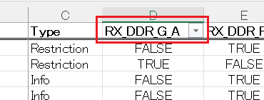
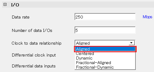
RX_DDR_G_AのGはglobal clockを意味します。

RX_DDR_G_AのAはAlignedを意味します。
同様に、
Rはfabric regional clock
CはCentered
DYNはDynamic
FAはFractional-Aligned
を指します。