- Semiconductor BusinessHOME
- Products and Services of Macnica,Inc.
-
technical information

-
Events and Seminars
- Handling Manufacturer
- Support
- Inquiry
- Click here to purchase products
- Semiconductor business e-mail magazine registration

THine Electronics Corporation Next-generation high-speed interface standard technology "V-by-One® HS plus Standard" compatible FPGA IP core
Overview
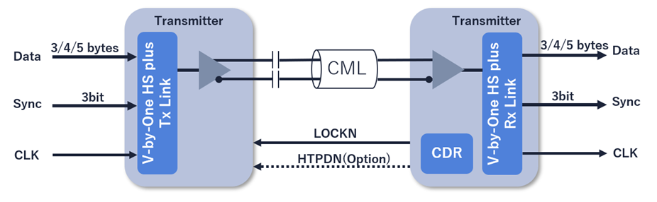
V-by-One® HS plus Tx/Rx IP is an IP for realizing transmission and reception of signals compatible with the latest "V-by-One® HS plus Standard" on Altera® FPGA.
Overview of V-by-One® HS plus Standard
V-by-One® HS plus is a next-generation high-speed interface standard technology proposed and formulated by THine Electronics, Inc. The main points are as follows:
- Maximum transmission speed of 8Gbps/lane
It is twice as fast as conventional technology and supports high resolution LCD and OLED TVs as well as high refresh rates for gaming. - Cable reduction and slimming
By reducing and streamlining the transmission paths inside the device, it contributes to reducing system costs and power consumption. - Ensuring backward compatibility
Two modes are defined: "HS Mode", which is backward compatible with the conventional V-by-One® HS, and "HS plus Mode", which enables transmission at up to 8Gbps/lane. - Improved user convenience
This is a next-generation high-speed interface standard that follows the basic protocol and design concept of the conventional V-by-One® HS and has a low barrier to adoption.
Features of this IP
Supported configurations
- Byte Mode
Supports 3-byte, 4-byte, or 5-byte modes. - Number of Lanes
Supports aggregation of up to 32 lanes. - backward compatibility
Both "HS Mode" and "HS plus Mode" are supported.
Transfer speed
- Up to 8.0 Gbps/lane
Other functions
- Test Pattern Mode
Supports PRBS7, PRBS9, K28.1, and V-by-One HS plus - Inter-lane deskew (Rx)
Up to 15 symbol clocks
IP release schedule (by supported FPGA)
Manufactured by Altera®
- Arria® 10 GX FPGA
- Cyclone® 10 GX FPGA
- Agilex™ 7 FPGA * Support is available for F-Tile products.
- Agilex™ 5 FPGA *Please contact us for details.
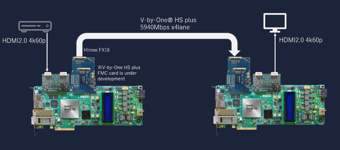
Demo configuration example