
![]()
![]() Narrow down by specifying conditions
Narrow down by specifying conditions
現在1888件がヒットしています。check

Difficulties in using SiC devices
The growing demand for high efficiency, high power density, and system simplicity has made silicon carbide (SiC) FETs an attractive choice for power engineers due to their fast switching speeds, low RDS(on), and high voltage ratings. It is
However, the faster switching speed of SiC devices results in longer ringing times, larger VDS spikes, and more EMI at high current levels. For engineers working in high-power applications such as EVs and renewable energy, this seeks to improve efficiency and maximize the potential of this advanced technology without adding unnecessary design complexity. sometimes a concern.
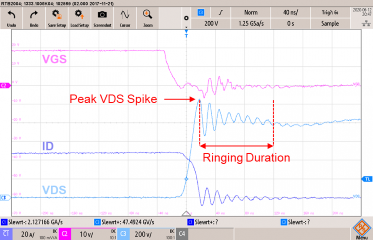
What are VDS spikes and ringing?
The root cause of VDS spikes and ringing is parasitic inductance. Looking at a typical turn-off waveform of a SiC MOSFET (Figure 1), the gate-to-source voltage (VGS) is 18V to 0V, the drain current (ID) is 50A at turn-off, and the bus voltage (VDS) is 800V. is. The faster switching speed of SiC MOSFETs results in higher VDS spikes and longer ringing times. A high VDS spike reduces the margin of the device to handle voltage sags due to conditions such as lightning or sudden load changes. Long ring times increase EMI. This phenomenon becomes more pronounced at high current levels.
traditional method
A standard solution to suppress EMI is to use a high gate resistance (RG) to lower the di/dt. However, this method introduces a trade-off between efficiency and EMI. In fact, using high RG dramatically increases switching losses.
Another solution is to reduce the stray inductance of the power loop. However, it requires redesigning the PCB layout and using smaller, less inductive packages. Additionally, there are limits to how much the PCB power loop area can be minimized, and there are safety regulations that set minimum spacing and clearance distances. Also, using a smaller package sacrifices thermal performance.
There are also filter designs to help meet EMI requirements and ease system trade-offs. Additionally, control methods can be used to reduce EMI. For example, frequency dithering techniques reduce EMI by spreading the power supply's noise spectrum.
new way
A more effective and efficient approach is to employ a simple RC snubber. This reduces design challenges and maximizes the capabilities of SiC devices. This simple solution effectively controls the duration of VDS spikes and ringing, improves efficiency over a wide load range, and shows negligible turn-off delay. Due to the faster dv/dt and additional C, the snubber displacement current is also higher. This means less overlap between ID and VDS during the turn-off transition.
Evidence of this can be seen using the double pulse test (DPT) to study the effect of snubbers. A half-bridge configuration with an inductive load. Both high side and low side use the same device. VGS, VDS, and ID are measured from the low-side device (Figure 2). A current transformer (CT) measures both the device current and the snubber current. Therefore, the measured switching loss includes both device switching loss and snubber loss.
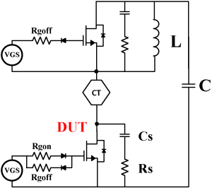
If a snubber is used, it is a 200pF capacitor in series with a 10Ω resistor across the drain and source of the SiCMOSFET.
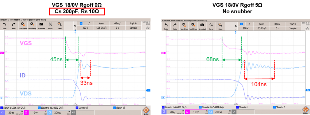
First, let's compare turn-off (Figure 3). For the same device in Figure 1, the waveform on the left uses an RC snubber and low RG(off), and the waveform on the right uses a high RG(off) but no snubber. Both methods limit the peak spike voltage of turn-off VDS. However, the snubber uses 33ns to dampen the ringing, while the ringing duration for high RG(off) exceeds 100ns. Also, the snubber has a shorter delay time than using a high RG(off). Snubbers are therefore more effective in controlling both the VDS turn-off spike and ring time at turn-off.
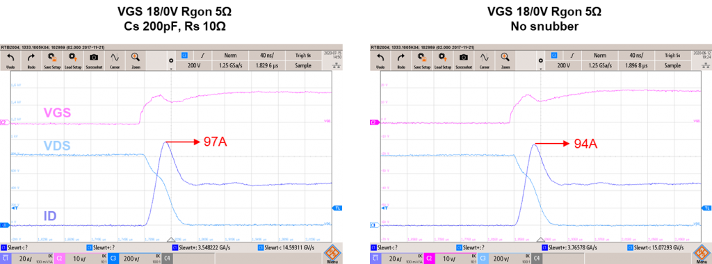
On the turn-on side (Figure 4), comparing the waveforms with an RC snubber and RG(on) of 5Ω to no snubber, we can see that the peak reverse recovery current (Irr) increases from 94A to 97A using a small snubber. I understand. Other than that, the effect on the turn-on waveform is negligible.
This suggests that snubbers are more effective than high RG(off) in controlling VDS spikes and ringing durations. But are snubbers more efficient? (Fig.5)
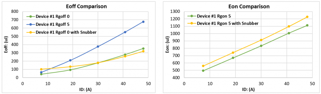
It can be seen that at 48A, a high RG(off) has more than twice the turn-off switching losses when using a low RG(off) snubber. Snubbers are therefore more efficient at turn-off as they allow faster switching while providing better control of VDS spikes and ringing.
Looking at the turn-on switching losses, the snubber slightly increases Eon by an average of 70µJ. Therefore, to fully estimate overall efficiency, Eoff and Eon must be summed and Etotal compared (Figure 6). It is clear that snubbers are more efficient above 18A when the device switches at full speed. For a 40mΩ device switching at 40A/40kHz, the switching loss difference between using high RG(off) and low RG(off) with a snubber is 11W per device.
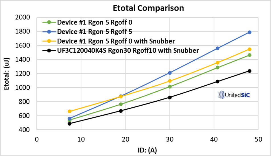
Therefore, we can conclude that a snubber is more effective and efficient than using a high RG(off). Entering the fourth generation of SiC devices, this simple design solution continues to provide even lower total switching losses while optimizing system power efficiency.
An application note on snubber circuits is also available.
Inquiry
If you have any questions regarding this article, please contact us below.
Qorvo manufacturer information top page
If you want to return to Qorvo manufacturer information Top, please click below.
