- 半導体事業HOME
- マクニカの製品・サービス
-
技術情報

-
イベント・セミナー
- 取扱メーカー
- サポート
- お問い合わせ
- 製品購入はこちら
- 半導体事業のメルマガ登録
![]()
![]() 条件を指定して絞り込む
条件を指定して絞り込む
現在2183件がヒットしています。check

はじめに
昨今、様々な場面でカメラを目にすることが多くなりました。
身近なところでは20年前にカメラ付き携帯電話が発売され、ゲーム機やPCにもカメラが付いていることが当たり前となりました。
また、自動車事故を減らす目的で自動車にもカメラが装着されることが当たり前となり、今ではカメラが装着されていない車を探すほうが大変となりました。
これらのカメラで使われている重要な半導体がイメージセンサーです。
一般的にCMOSイメージセンサーで取り込める光は人間の目で認識できる可視光領域から近赤外領域までの360nm~1100nmの範囲と言われています。
では、何故この領域の光が取り込めるのでしょうか?
その理由について説明します。
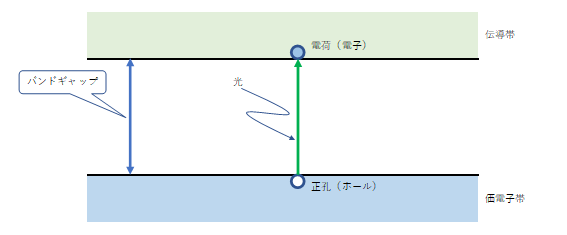
イメージセンサーは画素の中に埋め込まれている受光素子、フォトダイオードと呼ばれる部分で光を電荷に変えています。
これはCMOSイメージセンサーも今では見る機会が減りましたがCCDでも同じ仕組みで光を電荷に変えています。
この光を電荷に変える仕組みを光電効果と言い、光電効果には内部光電効果と外部光電効果の2種類があり、イメージセンサーは内部光電効果の仕組みを応用しています。
光電効果とは何か?
光電効果とは、光が物質面を照射したとき、その面から電子が外部に放出され、または物質内部の伝導電子数が増加する現象を言います。
その光電効果の中で外部光電効果は光の持つエネルギーによって、物質が持つ電荷(電子)が外部に放出される現象、
内部光電効果は同じく光の持つエネルギーによって、物質(主に半導体)の内部で電荷が発生し、起電力などが生じる現象を言います。
内部光電効果を起こすためには価電子帯から伝導帯へ電子を励起させる必要があります。
このためには光のエネルギーが半導体の持つバンドギャップ(禁止帯、禁制帯とも言います)以上であることが条件です。
その関係式は、Epを光のエネルギー(eV)、Egをバンドギャップ(eV)、λを波長 (nm) として、次の式に表されます。
Ep = 1240/λ
Ep > Eg
波長λ(nm)毎で計算すると次のようになります。
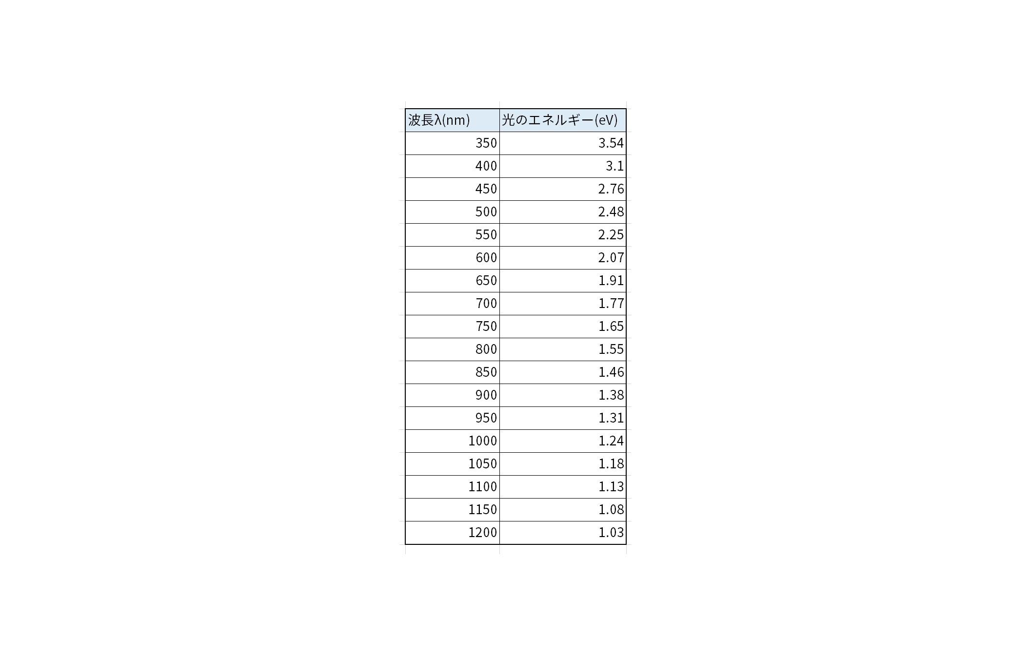
半導体の持つバンドギャップ以上のエネルギーを持つ光を照射することによって価電子帯から電荷(電子)を励起することができます。
逆を言うと、バンドギャップ以下のエネルギーを持つ光を照射しても、価電子帯から電荷(電子)を励起することができません。
広く使われているシリコン(Si)のバンドギャップは約1.1eVで、Si系半導体で光電効果を起こすためには1.1eV以上の光のエネルギーが必要になります。
このため、1.1eV以上の光エネルギーを得るためには波長1100nm以下の光である必要があり、このためSi系半導体を使っているイメージセンサーでは1100nm以下の光を取り込める仕様となっています。
バンドギャップがより狭い材料を選択すれば1100nm以上の中赤外~遠赤外の光を取り込むことが可能となり、例えばGe(ゲルマニウム)は0.67eVで先ほどの式に当てはめると1850nmまでの光を取り込むことができます。
また、InGaAs(インジウムガリウムヒ素、インガスとも言います)は1.4eVのGaAsと0.36eVのInAsを組み合わせた3元混晶半導体であり、その組成比によってバンドギャップを変えることができ、見たい光の波長に応じて組成比を変えて活用しています。
さいごに
日頃何気なく使っているデジタルカメラやスマートフォンのカメラが光というエネルギーを何故取り込めて眼に見える画像などの形にしている入り口を説明しました。
この記事がCMOSイメージセンサーの理解を深める一助となればと思います。
お問い合わせ
本記事にて紹介した製品に、ご興味がある方は、ぜひお問い合わせください。
オンセミ メーカー情報Topへ
オンセミ メーカー情報Topに戻りたい方は以下をクリックしてください。