- Semiconductor BusinessHOME
- Products and Services of Macnica,Inc.
-
technical information

-
Events and Seminars
- Handling Manufacturer
- Support
- Inquiry
- Click here to purchase products
- Semiconductor business e-mail magazine registration
![]()
![]() Narrow down by specifying conditions
Narrow down by specifying conditions
現在2169件がヒットしています。check

Introduction
Power semiconductor manufacturers develop new packages every few years and introduce them to the market. New package requirements include miniaturization and minimizing package parasitics and on-resistance. In addition, most of the conventional packages are drain-down packages, in which the drain faces the bottom surface of the package.
This time, I will introduce the merits of using the source-down package, which is a new package from ONSEMI.
The main benefits are:
・ Improved heat dissipation
・ Simplification of layout ・Space saving
Details are explained in the next section.
Improved heat dissipation
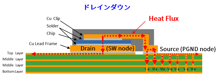
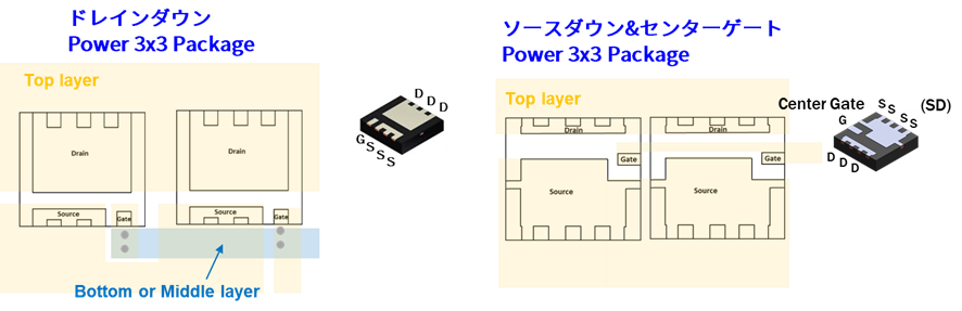
The figure below shows the internal structure of the drain down package and the side view of the substrate. Heat Flux (red arrow) is the heat dissipation path. Since the drain side switches at a high voltage, it is not possible to open vias in other layers, so there is only a heat dissipation path in the pattern on the substrate surface (top layer).
Also, it is necessary to open a via on the source side, but since the pad on the source part is small, the area where the via can be opened directly under the source pad is narrow. Basically, heat escapes to the source side, but since it passes through vias under the pattern (wiring) of the top layer, the heat dissipation path is also long.
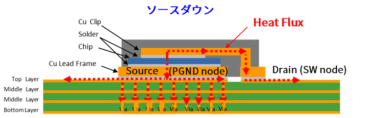
Source-down packages, on the other hand, can avoid this problem. By adopting a source-down package, it is possible to place vias in a wide area directly under the source pad. Since the source side has a stable potential, heat can be released to each layer through vias. Therefore, heat can be released to the board in the shortest distance.
Simplified layout and space saving
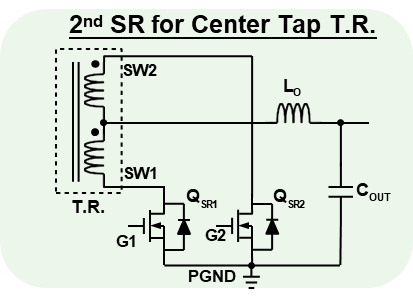
When used in a secondary-side synchronous rectification circuit such as ACDC or in a step-down converter
An example of a general secondary-side synchronous rectification circuit is shown below.
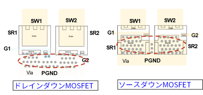
In the circuit above, if a conventional drain-down package is used for the MOSFETs QSR1 and QSR2, as shown in the left figure below, in order to improve the heat dissipation characteristics, a via should be added to the source wiring part of the top layer other than the part where the device is mounted. Therefore, the range of usable board area becomes large.
On the other hand, when a source-down package is used, it is possible to improve heat dissipation by inserting vias directly under the source pad as shown on the right in the figure below, and it is also possible to reduce the board area used.
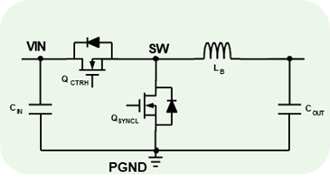
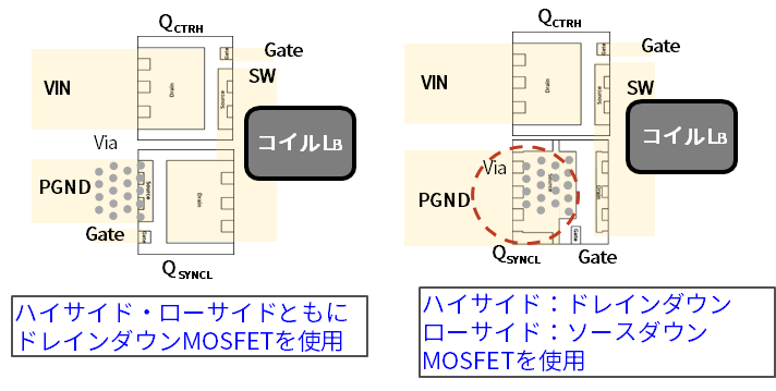
In step-down converters, etc., by using the drain down on the high side and the source down on the low side, it is possible to save the board area and widen the GND pattern in the same way as above, resulting in good heat dissipation. Become. The figure on the right is a typical circuit example of a buck converter.
The left figure below shows the case of using drain-down MOSFETs on both the high and low sides, and the right figure below shows the case of using drain-down MOSFETs on the high side and source-down MOSFETs on the low side.
For parallel connection
Paralleling devices is required to reduce the on-resistance. In a general drain-down package, it is difficult to directly connect the gate signal wiring in the top layer directly under the device. Besides the layer, one more layer should be used. (Fig. left, gate signal is blue)
On the other hand, the source-down package uses a center-gate structure with the gate in the middle of the drain and source, as shown in the right figure below. A center-gate structure may also allow the gate signals of paralleled devices to be routed without using a separate layer. Therefore, placement and layout of devices connected in parallel are easy.
Application example
・DCDC converter
・Secondary side synchronous rectification
・Motor drive/three-phase motor control
・SMPS
・Battery management system
Inquiry
If you are interested in any of the products introduced in this article, please feel free to contact us.
Onsemi Manufacturer information Top
If you want to go back to ONSEMI Manufacturer Information Top, please click below.